Lamination for Printed Photomask

a printed circuit board and photomask technology, applied in the field of printed circuit board manufacturing, can solve the problems of manufacturers using expensive alignment tools and fixtures, manufacturers reducing the cost of manufacturing, so as to avoid adding to the cost and time of production.

Inactive Publication Date: 2009-05-14
PALO ALTO RES CERNTER
View PDF16 Cites 22 Cited by
  • Summary
  • Abstract
  • Description
  • Claims
  • Application Information

AI Technical Summary

Benefits of technology

[0015]Accordingly, the present invention is directed to methods for forming a printed circuit board which masks regions around through holes such that the sidewalls of the through-holes are not exposed to UV light prior to development of photo-sensitive solder mask material. In a photo-sensitive material-based ...

Problems solved by technology

However, there remains pressure on manufacturers to reduce cost of manufacturing.
One significant expense in the manufacturing process is the mask manufacturing.
This alignment requires manufacturers to use expensive alignment tools and fixtures during device manufacturing and adds to the production time for such parts.
The problem arises in ...

Method used


Image

  • Lamination for Printed Photomask
  • Lamination for Printed Photomask
  • Lamination for Printed Photomask

Examples


Embodiment Construction

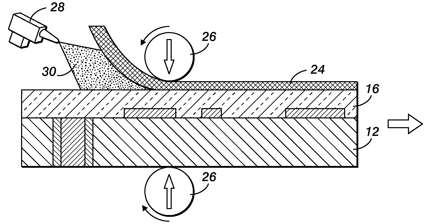
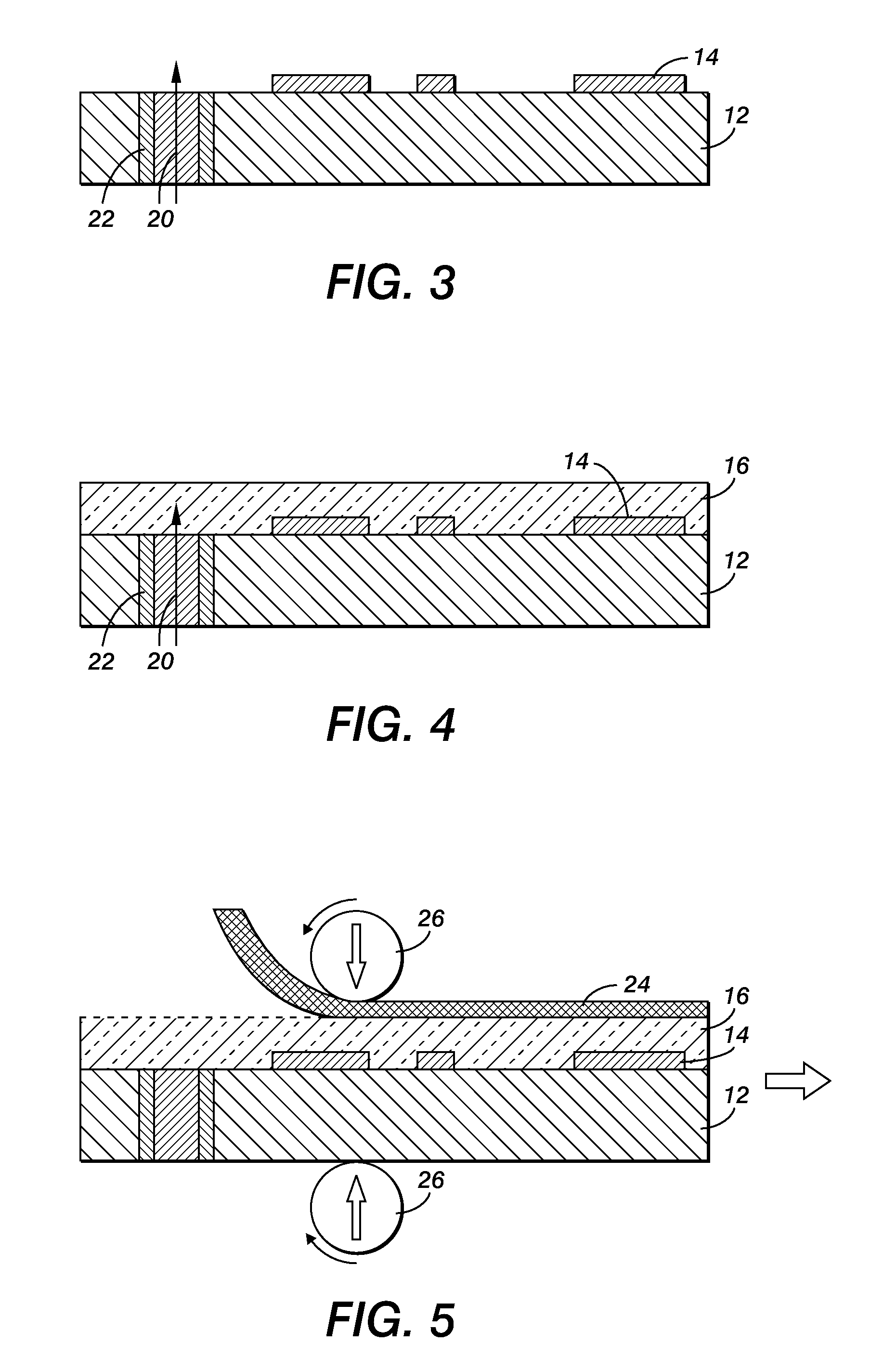
[0037]Described in the following section are specific steps for the formation of a printed photomask, and the production of structures formed with said mask. The printed photomask is formed on a thin film carrier, temporarily applied to the structure being masked. An improved process for the formation of printed circuit boards is thereby enabled.

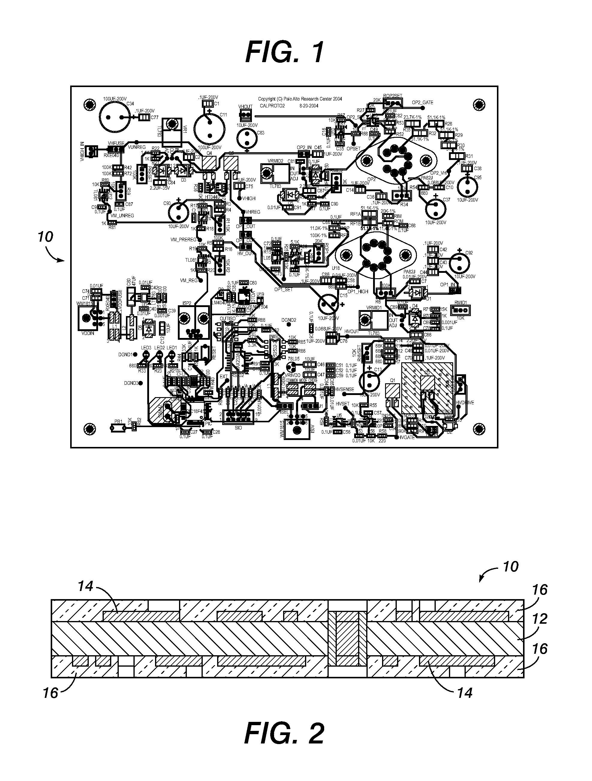
[0038]With reference to FIGS. 1 and 2, there is shown therein an example of a printed circuit board 10 of a type which may be manufactured according to the present invention. Printed circuit board (or PCB) 10 consists of a substrate 12 such as a woven / laminated fiberglass material. The substrate is rigid and can be drilled, cut or machined. Applied to the substrate is a patterned network of conductive electrical interconnections, for example traces 14. While beyond the scope of this disclosure, traces 14 are typically photolithographically patterned copper applied to the surface of substrate 12 as well understood in the art.

[0039]Applied ove...


PUM


Abstract

A method for masking regions of photoresist in the manufacture of a soldermask for printed circuit boards is disclosed. Following application of photoresist over patterned traces on a substrate, a sheet-like thin film is applied over the photosensitive material. The thin film may adhere to the photosensitive material by way of the adhesive state of the photosensitive material or by way of an adhesive applied to the photosensitive material or the thin film or carried by the thin film. Digital mask printing may proceed on the surface of the thin film. The photosensitive material may then be exposed through the printed photomask, the thin film (with photomask) removed, and the photosensitive material developed.

Description

BACKGROUND OF THE INVENTION[0001]1. Field of the Invention[0002]The present invention is related to the manufacture of printed circuit boards, and more particularly to a method of masking regions of a plated substrate during a pre-development expose phase of manufacturing.[0003]2. Description of the Prior Art[0004]A printed circuit board (“PCB”) is a rigid or semi-flexible structure designed to have electrical or electromechanical components attached thereto. PCBs may be found in virtually all of the electronic devices with which we come into contact today. The PCB itself typically consists of a non-conductive substrate having a number of patterned conductive interconnections, or traces, formed on one of both sides thereof. The traces permit electrical interconnection of the components attached to the PCB. Typically, both sides of the non-conductive substrate are first plated in copper. The copper is selectively removed, remaining only where electrical interconnection is desired. An...

Claims


Application Information

Patent Timeline
IPC IPC(8): G03F7/26H05K1/02
CPCH05K3/0023H05K3/0082H05K3/28H05K3/42H05K2203/0783H05K2203/013H05K2203/0191H05K2203/0551H05K2201/09545
Inventor SHRADER, ERICSRINIVASAN, UMACRAWFORD, CLARKLIMB, SCOTT
Owner PALO ALTO RES CERNTER
Why Eureka
Try Eureka