
Laser beam machining apparatus

a laser beam and machining technology, applied in the direction of instruments, manufacturing tools, spectrum investigation, etc., can solve the problems of difficult to stop the irradiation of pulsed laser beams, low productivity of hole drilling by drilling, and melting of bonding pads

Inactive Publication Date: 2009-05-21
DISCO CORP
View PDF30 Cites 48 Cited by
  • Summary
  • Abstract
  • Description
  • Claims
  • Application Information

AI Technical Summary

Benefits of technology

[0008]Accordingly, it is an object of the present invention to provide a laser beam machining apparatus with which via holes reaching bonding pads can be formed in a substrate of a wafer, without forming holes in the bonding pads.
[0013]In the laser beam machining apparatus according to the present invention, the plasma detecting means which includes the plasma receiving means for receiving a plasma generated by irradiation of a work with a pulsed laser beam from laser beam irradiation means and spectrum analyzing means for analyzing the spectrum of the plasma received by the plasma receiving means, and the control means which determines the material of the work on the basis of a spectrum analysis signal from the spectrum analyzing means of the plasma detecting means and controls the laser beam irradiation means, are provided. Therefore, for example in the case where the substrate of a wafer provided with bonding pads on the face side is irradiated with a laser beam from the back side so as to provided the substrate with laser beam-machined holes reaching the bonding pads, it is possible to detect that the laser beam-machined holes formed in the substrate have just reached the bonding pads, based on the spectrum analysis signal from the spectrum analyzing means. Therefore, the irradiation of the wafer with the laser beam can be stopped upon detection of the reaching of the laser beam-machined holes to the bonding pads, and, accordingly, the bonding pads can be prevented from melting with the result of formation of holes.

Problems solved by technology

However, the through-holes (via holes) formed in the semiconductor wafer has a diameter as small as 90 to 300 nm, and the formation of the holes (boring) by drilling is therefore low in productivity.
Meanwhile, in the case where the via holes reaching the bonding pads are formed by irradiation with a pulsed laser beam from the back side of the substrate, it is difficult to stop the irradiation with the pulsed laser beam at the time when the via holes formed in the substrate have just reached the bonding pads.
As a result, there is the problem that the bonding pads may be melted, and holes may be formed in the bonding pads, under the irradiation with the pulsed laser beam.

Method used


Image

  • Laser beam machining apparatus
  • Laser beam machining apparatus
  • Laser beam machining apparatus

Examples


Embodiment Construction

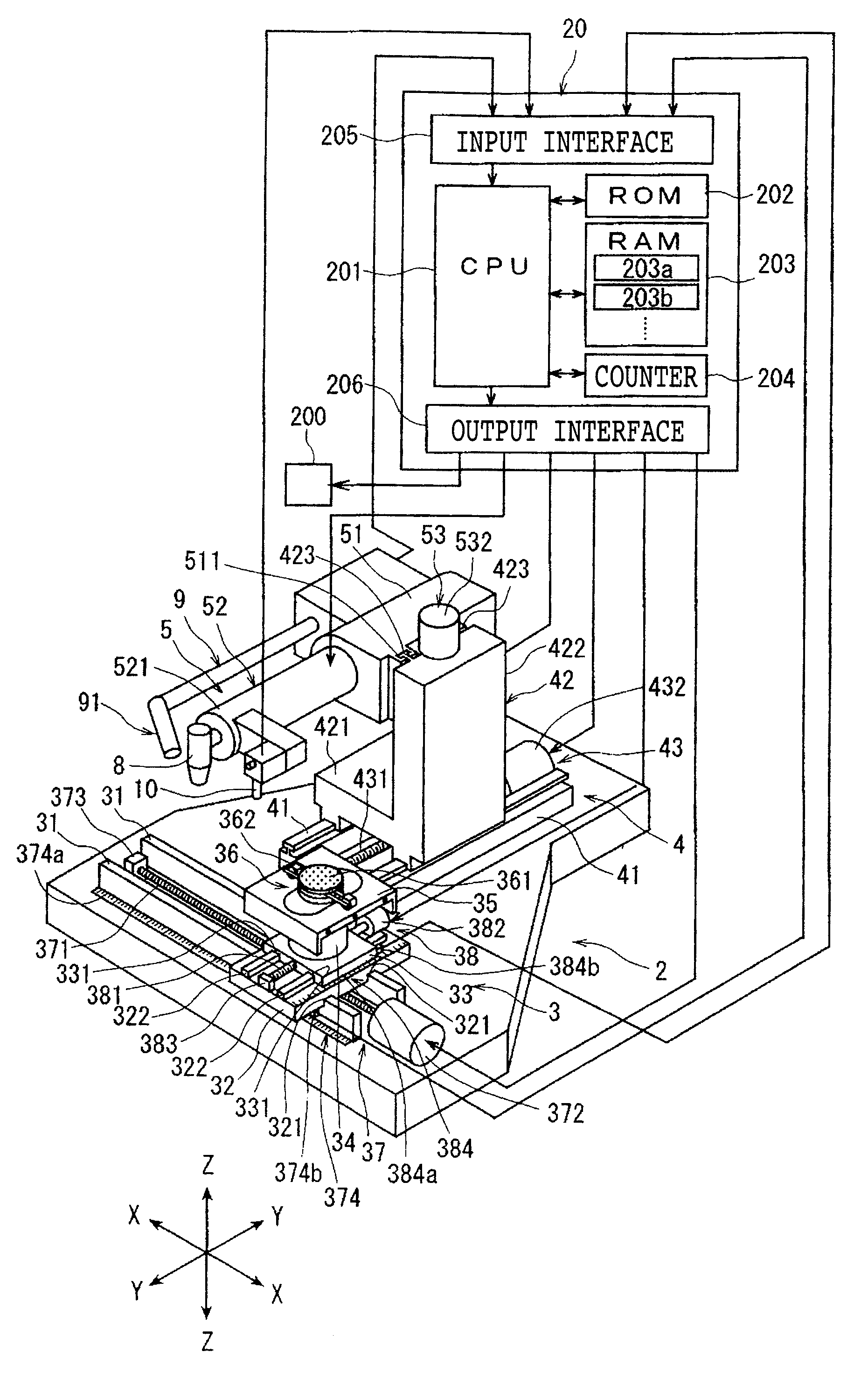
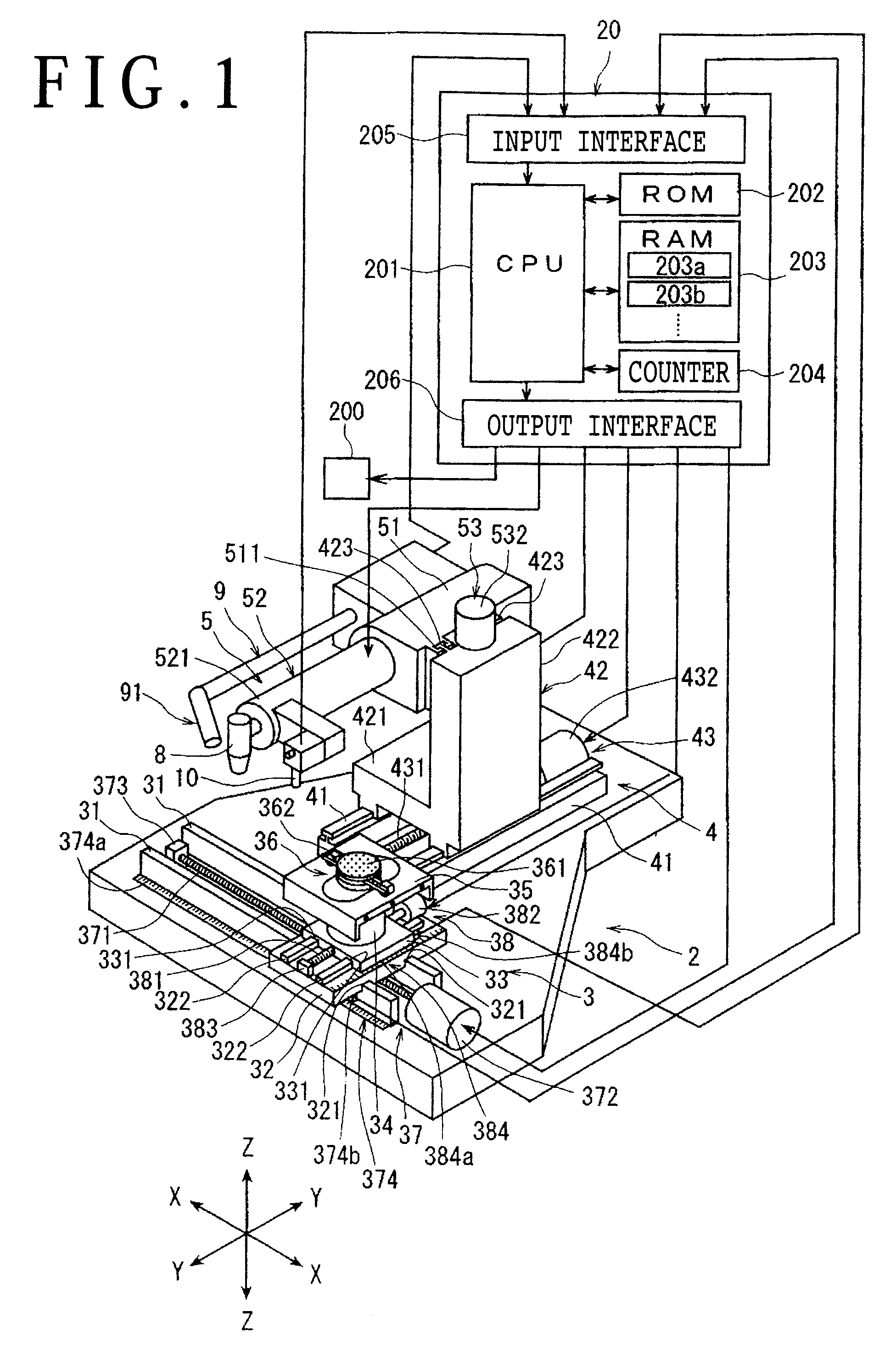
[0026]Now, a preferred embodiment of the laser beam machining apparatus configured according to the present invention will be described more in detail below, referring to the attached drawings. FIG. 1 shows a perspective view of a laser beam machining apparatus configured according to the present invention. The laser beam machining apparatus shown in FIG. 1 includes: a stationary base 2; a chuck table mechanism 3 for holding a work, disposed on the stationary base 2 so as to be movable in a machining feed direction indicated by arrow X (X-axis direction); a laser beam irradiation unit support mechanism 4 disposed on the stationary base 2 so as to be movable in an indexing feed direction indicated by arrow Y (Y-axis direction) orthogonal to the direction indicated by arrow X (X-axis direction); and a laser beam irradiation unit 5 disposed on the laser beam irradiation unit support mechanism 4 so as to be movable in a direction indicated by arrow Z (Z-axis direction).

[0027]The chuck t...


PUM

PropertyMeasurementUnit
Wavelengthaaaaaaaaaa

Abstract

A laser beam machining apparatus including a chuck table for holding a wafer, and a laser beam irradiation unit for irradiating the wafer held on the chuck table with a pulsed laser beam. The laser beam machining apparatus further includes a plasma detecting part which includes a plasma receiving part for receiving a plasma generated by irradiation of the work with the laser beam radiated from the laser beam irradiation unit, and a spectrum analyzing part for analyzing the spectrum of the plasma received by the plasma receiving part; and a controller for determining the material of the work on the basis of a spectrum analysis signal from the spectrum analyzing part of the plasma detecting part and for controlling the laser beam irradiation unit.

Description

BACKGROUND OF THE INVENTION[0001]1. Field of the Invention[0002]The present invention relates to a laser beam machining apparatus for forming a laser beam machined hole in a work such as a semiconductor wafer.[0003]2. Description of the Related Art[0004]In the semiconductor device manufacturing process, a plurality of regions are demarcated in a face-side surface of a roughly circular disk-shaped semiconductor wafer by planned dividing lines called streets, and devices such as ICs and LSIs are formed in the thus demarcated regions. Then, the semiconductor wafer is cut along the streets so as to divide the regions provided therein with the devices, thereby manufacturing individual semiconductor chips.[0005]In order to realize smaller apparatus sizes and higher functions, a module structure in which a plurality of devices are stacked and bonding pads provided on the stacked devices are connected has been put to practical use. The module structure has a configuration in which the semic...

Claims


Application Information

Patent Timeline
IPC IPC(8): B23K26/00B23K26/382B23K26/40B23K101/40
CPCB23K26/032B23K26/0853G01J3/443H01L21/67253G01N2021/8416G01N2201/0697G01N21/73H01L21/3065
Inventor ASANO, KENJIMORIKAZU, HIROSHITAKAHASHI, KUNIMITSU
Owner DISCO CORP
Learn More