Vertical transitions, printed circuit boards therewith and semiconductor packages with the printed circuit boards and semiconductor chip

Active Publication Date: 2009-05-28
NEC CORP
View PDF11 Cites 57 Cited by
  • Summary
  • Abstract
  • Description
  • Claims
  • Application Information

AI Technical Summary

Benefits of technology

[0084]An exemplary advantage according to the invention of the above constitution is capable of reducing the influence by resonances of parallel plate modes etc. with signal propagating in the vertical transition and is capable of improving highly the electrical performance and the shielding properties in the wide frequency band of the vertical transition in a multilayer PCB.
[0085]In addition, it is particularly important to use the above closed ground stripline in the above constitution at a

Problems solved by technology

These transitions have usually poor-defined wave guiding properties that leads to problems in controlling characteristic impedance and high leakage, especially, at higher frequencies.
At higher frequencies the single signal v

Method used


Image

  • Vertical transitions, printed circuit boards therewith and semiconductor packages with the printed circuit boards and semiconductor chip
  • Vertical transitions, printed circuit boards therewith and semiconductor packages with the printed circuit boards and semiconductor chip
  • Vertical transitions, printed circuit boards therewith and semiconductor packages with the printed circuit boards and semiconductor chip

Examples


first exemplary embodiment

A First Exemplary Embodiment

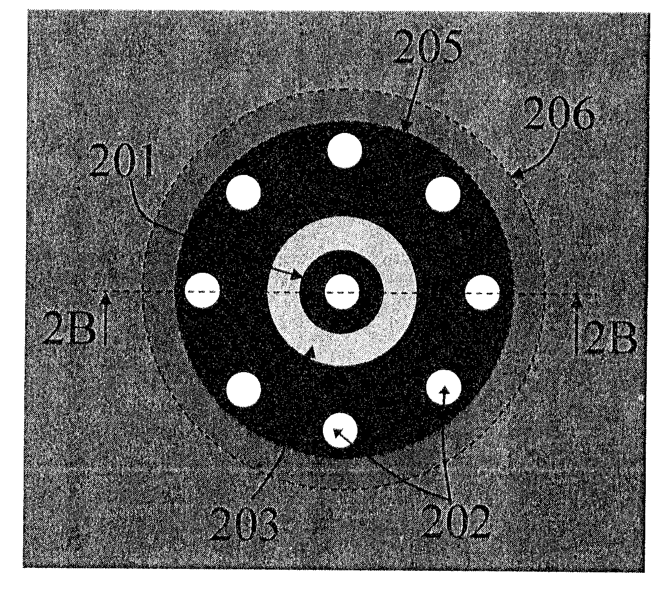
[0142]Referring to the drawings, FIGS. 4A and 4B show a vertical transition with a round arrangement of ground vias 202 of a first exemplary embodiment. The vertical transition is embedded in a 12-conductor-layer PCB.

[0143]FIG. 4B shows a cross-sectional view of a vertical transition (in a direction of a dotted line 2B in FIG. 4A), the arrangement of conductor layers of the PCB separated by an isolating material is as follows: Ground planes are 2nd, 4th, 6th, 7th, 9th, and 11th layers; Power supply plane is 5th layer; Signal planes are 1st, 3rd, 8th, 10th, and 12th layers. The single signal via 201 is separated electrically from conductor planes of the PCB by a clearance hole 203.

[0144]FIG. 4A shows a top view of a power supply layer which is 5th layer of a vertical transition. The number of ground vias 202 is 8. In addition, although the number of ground vias 202 is 8 here, the number can be selected as necessary.

[0145]To improve the shielding properties...

second exemplary embodiment

A Second Exemplary Embodiment

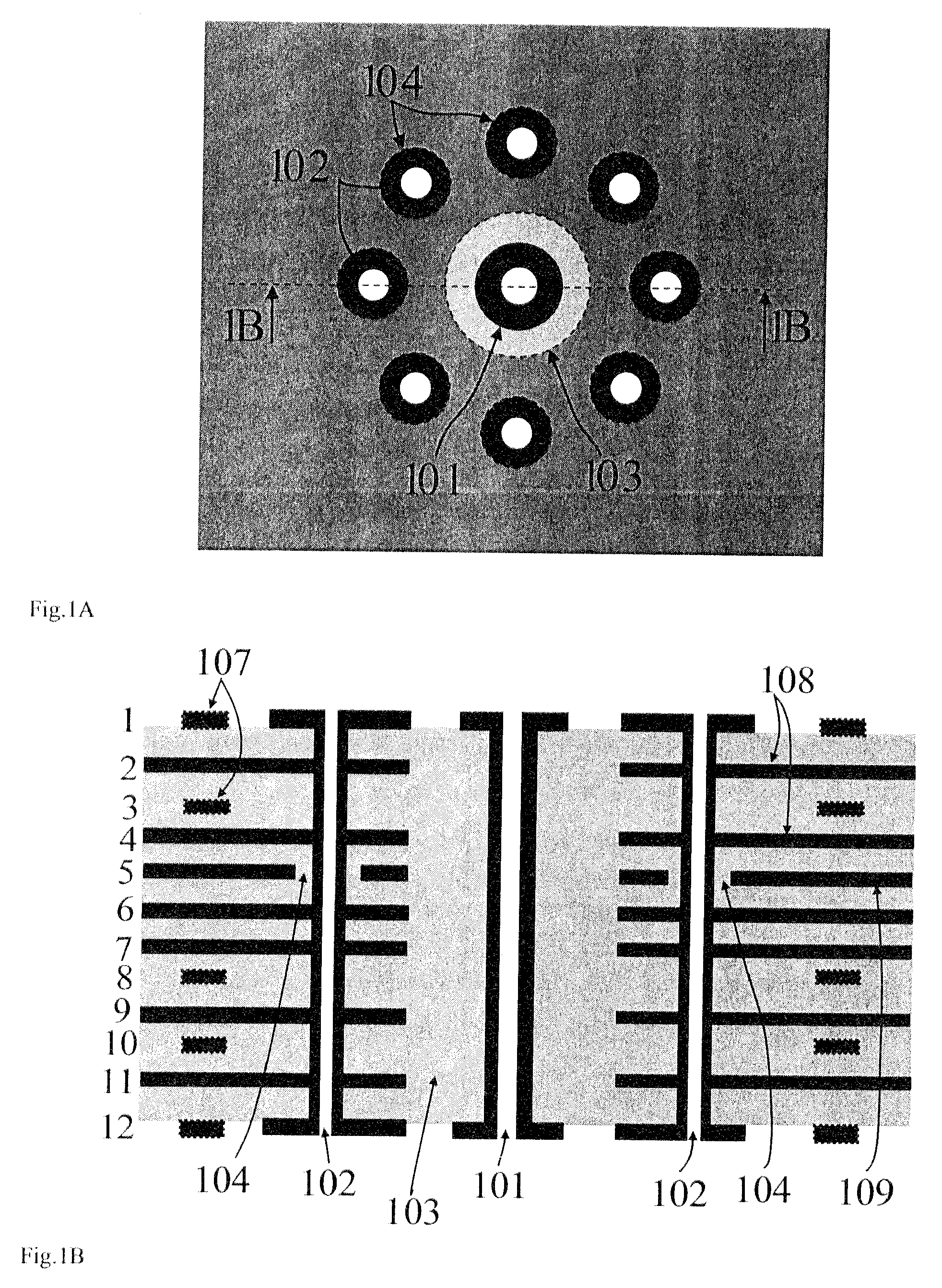
[0154]In FIGS. 6A and 6B a vertical transition with another arrangement of ground vias 402 such as square one is shown. This vertical transition is embedded in a 10-conducter-layer PCB which serves as an example of multilayer PCBs.

[0155]FIG. 6B shows a cross-sectional view of a vertical transition (in a direction of a dotted line 4B in FIG. 6A), the arrangement of conductor layers of the PCB separated by an isolating material is as follows: Ground planes are 2nd, 4th, 6th, 7th and 9th layers; Power supply plane is 5th layer; Signal planes are 1st, 3rd, 8th and 10th layers. The single signal via 401 is separated from conductor planes of the PCB by a clearance hole 403.

[0156]FIG. 6A shows a top view of a power supply layer which is 5th layer of a vertical transition. The vertical transition is formed by a signal via 401, an assembly of ground vias 402 around the signal via 401, ground plates 408 from conductor layers connected to the ground vias 402, close...

third exemplary embodiment

A Third Exemplary Embodiment

[0157]In FIGS. 7A and 7B a vertical transition with the same arrangement of ground vias as in FIGS. 6A and 6B is shown. This vertical transition is also embedded in a 10-conducter-layer PCB which has the same constitution as that in FIGS. 6A and 6B.

[0158]FIG. 7B shows a cross-sectional view of a vertical transition (in a direction of a dotted line 5B in FIG. 7A).

[0159]FIG. 7A shows a top view of a power supply layer which is 5th layer of a vertical transition. The vertical transition is formed by a signal via 501, an assembly of ground vias 502 around the signal via 501, ground plates 508 from conductor layers connected to the ground vias 502, closed ground stripline 505 connecting the ground vias in turn, and an isolating slot 506 between said ground stripline and power supply layer 509 of the PCB. The number of ground vias 502 is 8. In addition, although the number of ground vias 502 is 8 here, the number can be selected as necessary. However a clearanc...


PUM


Abstract

Provided are vertical transitions which have the high electrical performance and the high shielding properties in the wide frequency band in a multilayer PCB, printed circuit boards with the vertical transitions and semiconductor packages with the printed circuit boards and semiconductor chips. In vertical transitions for a multilayer PCB, a wave guiding channel is a conductor which includes at least more than one of signal vias 201, an assembly of ground vias 202 surrounding the signal via, ground plates from conductor layers of the PCB connected to the ground vias, closed ground striplines 205 connecting the ground vias and power supply layer.

Description

TECHNICAL FIELD[0001]The present invention relates to multilayer printed circuit board technology, and more particularly, relates to vertical transitions connecting circuits disposed at different planar conductor layers of a multilayer printed circuit board (hereinafter referred to a multilayer PCB), printed circuit boards with the vertical transitions and semiconductor packages with the printed circuit boards and semiconductor chips.BACKGROUND ART[0002]A multilayer PCB usually comprises a number of planar conductor layers used for signal, ground and power supplies where the conductor layers are isolated by a material. Planar interconnect circuits embedded in the PCB can be developed on the base of transmission lines such as microstrip lines, strip lines, coplanar lines, and slot lines which have typically low leakage losses and well-defined characteristic impedance. These properties of planar transmission lines give a possibility to develop high-performance and matched interconnect...

Claims


Application Information

Patent Timeline
IPC IPC(8): H05K1/16H05K1/00
CPCH01L23/49827H01L2924/01087H01L2223/6622H01L2224/16H01L2924/01004H01L2924/01057H01L2924/3011H01L2924/3025H05K1/0222H05K1/115H05K1/116H05K3/429H05K2201/093H05K2201/09618H05K2201/09636H05K2201/09663H05K2201/09718H01L23/49838H01L2224/16235
Inventor KUSHTA, TARASNARITA, KAORU
Owner NEC CORP
Why Eureka
Try Eureka