Non-Volatile Memory Device with Improved Immunity to Erase Saturation and Method for Manufacturing Same

a non-volatile memory and memory device technology, applied in the direction of semiconductor devices, basic electric elements, electrical apparatus, etc., can solve the problems of affecting the efficiency of the control gate, the use of the p-type polysilicon control gate, and the tendency to change the effective work function towards midgap, etc., to achieve the effect of improving the immunity to erase saturation

Inactive Publication Date: 2009-05-28
SAMSUNG ELECTRONICS CO LTD +1
View PDF6 Cites 19 Cited by
  • Summary
  • Abstract
  • Description
  • Claims
  • Application Information

AI Technical Summary

Benefits of technology

[0005]Provided is a non-volatile memory device with improved immunity to eras

Problems solved by technology

The same problem arises in charge trapping non-volatile memory cells in which charge is stored in a charge trapping gate and the upper dielectric is called the blocking dielectric.
However, metal gates are difficult to integrate in a conventional process flow.
In addition, they show a tendency to change

Method used


Image

  • Non-Volatile Memory Device with Improved Immunity to Erase Saturation and Method for Manufacturing Same
  • Non-Volatile Memory Device with Improved Immunity to Erase Saturation and Method for Manufacturing Same
  • Non-Volatile Memory Device with Improved Immunity to Erase Saturation and Method for Manufacturing Same

Examples


Embodiment Construction

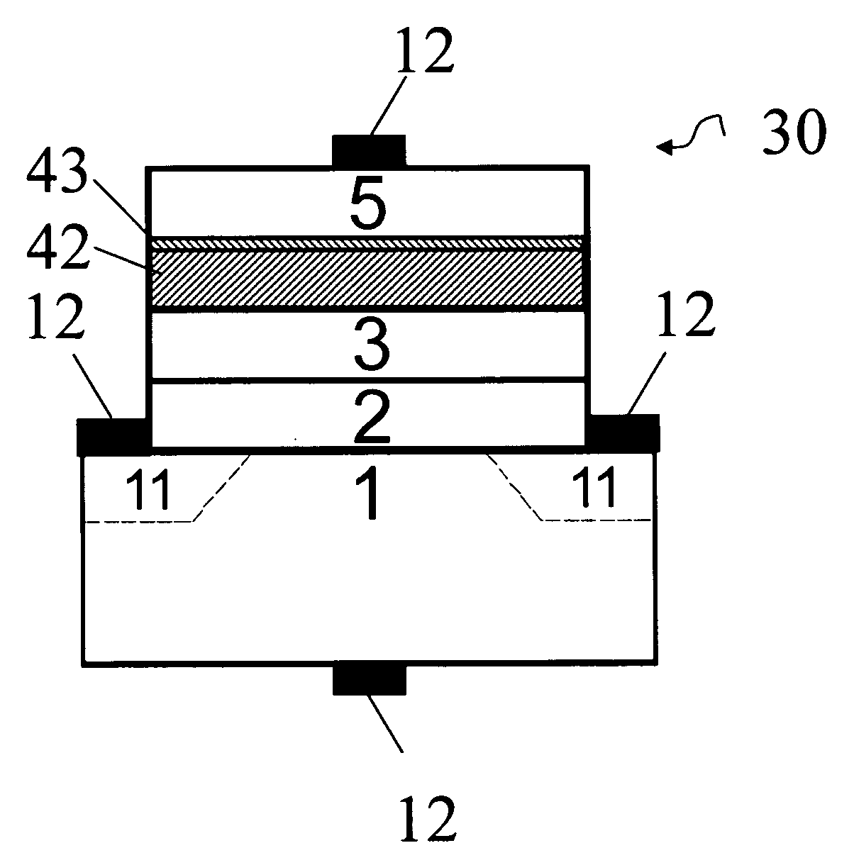
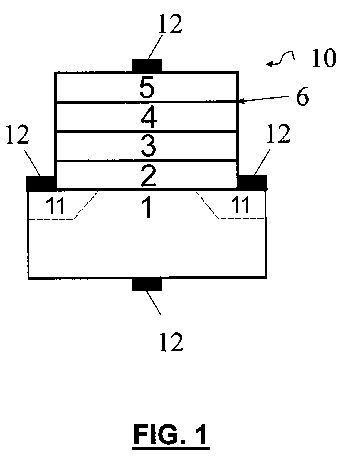
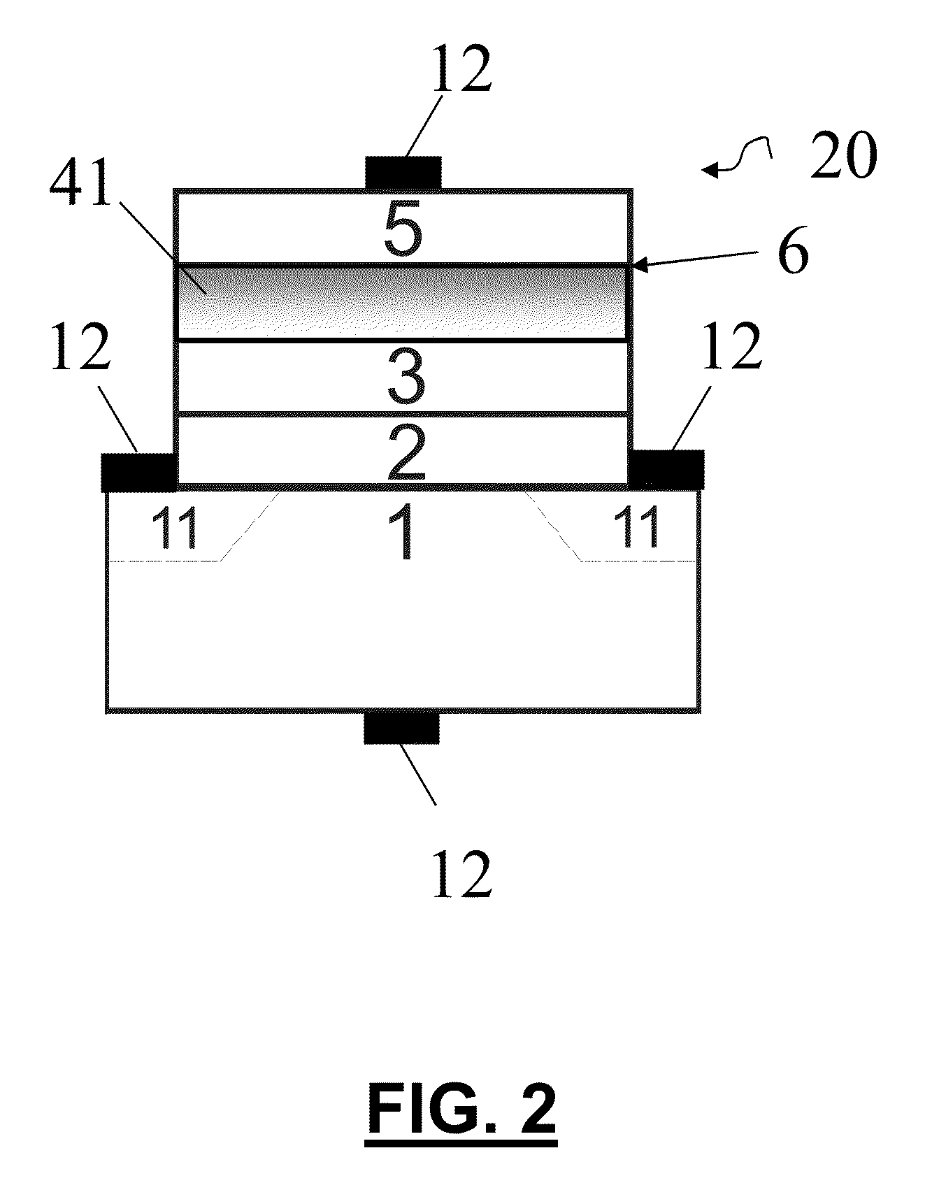
[0020]FIGS. 1-3 show three exemplary embodiments of non-volatile memory cells 10, 20, 30 according to the invention, each comprising a substrate with a channel 1 in between two doped regions 11 (source and drain), a first dielectric 2 on top of the channel 1, a silicon floating gate 3 on top of the insulating layer 2, a second dielectric 4, 41, 42-43 on top of the silicon floating gate 3 and a control gate 5 on top of the second dielectric. The first dielectric is the so-called tunnel dielectric and the second dielectric is the so-called interpoly dielectric. Each of the layers 2-5 may in itself be a single layer or a stack of different layers having substantially the same functionality as the respective single layer which the stack replaces. Contacts 12 are provided at the doped regions 11, at the bottom of the substrate 1 and on top of the control gate 5.

[0021]The embodiments may also be applied in charge trapping non-volatile memory cells in which charge is stored in a charge tra...


PUM


Abstract

A non-volatile memory device having a control gate on top of the second dielectric (interpoly or blocking dielectric), at least a bottom layer of the control gate in contact with the second dielectric being constructed in a material having a predefined high work-function and showing a tendency to reduce its work-function when in contact with a group of certain high-k materials after full device fabrication. At least a top layer of the second dielectric, separating the bottom layer of the control gate from the rest of the second dielectric, is constructed in a predetermined high-k material, chosen outside the group for avoiding a reduction in the work-function of the material of the bottom layer of the control gate. In the manufacturing method, the top layer is created in the second dielectric before applying the control gate.

Description

CROSS-REFERENCE TO RELATED APPLICATIONS[0001]This application claims priority to European Patent Application No. 07121292.2 filed Nov. 22, 2007 and U.S. Provisional Application Ser. No. 60 / 990,130 filed Nov. 26, 2007, the contents of which are incorporated by reference herein in its entirety.TECHNICAL FIELD OF THE INVENTION[0002]The present invention relates to a non-volatile memory device and a method for manufacturing a non-volatile memory device.BACKGROUND OF THE INVENTION[0003]Erase saturation refers to the inability to erase a floating gate memory cell by removing charge from the floating gate to the Si channel through the tunnel oxide. This effect occurs because the parasitic current injected from the control gate towards the floating gate through the interpoly dielectric. The same problem arises in charge trapping non-volatile memory cells in which charge is stored in a charge trapping gate and the upper dielectric is called the blocking dielectric.[0004]A way to avoid erase ...

Claims


Application Information

Patent Timeline
IPC IPC(8): H01L21/28H01L29/792
CPCH01L21/28273H01L29/7881H01L29/513H01L21/28282H01L29/40114H01L29/40117
Inventor GOVOREANU, BOGDANYU, HONGYUCHO, HAG-JU
Owner SAMSUNG ELECTRONICS CO LTD
Why Eureka
Try Eureka