Semiconductor integrated circuit

a technology of integrated circuits and semiconductors, applied in semiconductor/solid-state device testing/measurement, pulse techniques, instruments, etc., can solve the problems of large number of fuses and noise propagation, and achieve the effect of reducing the number of pads and increasing the inspection efficiency of the tes

Inactive Publication Date: 2009-05-28
LONGITUDE SEMICON S A R L
View PDF3 Cites 0 Cited by
  • Summary
  • Abstract
  • Description
  • Claims
  • Application Information

AI Technical Summary

Benefits of technology

[0007]To increase inspection efficiency of a prove test, there is a request to reduce further the number of pads which come in contact with probes. It is possible to connect plural power supply pads to each other. However, when the power supply pads with different usage are simply connected to each other with an aluminum wire or the like, there is possibility that a problem of the noise propagation is caused after a semiconductor circuit is turned into a finished product.

Problems solved by technology

However, when the power supply pads with different usage are simply connected to each other with an aluminum wire or the like, there is possibility that a problem of the noise propagation is caused after a semiconductor circuit is turned into a finished product.
Consequently, in such a case, there is a problem that it is necessary to blow the large number of the fuses afterwards.
In such a case, if the increased current, which is relatively large, is continue to be supplied to the probe, especially on a high temperature condition, there is a possibility of a following problem.

Method used


Image

  • Semiconductor integrated circuit
  • Semiconductor integrated circuit
  • Semiconductor integrated circuit

Examples


Embodiment Construction

[0017]The invention will be now described herein with reference to illustrative embodiments. Those skilled in the art will recognize that many alternative embodiments can be accomplished using the teachings of the present invention and that the invention is not limited to the embodiments illustrated for explanatory purposes.

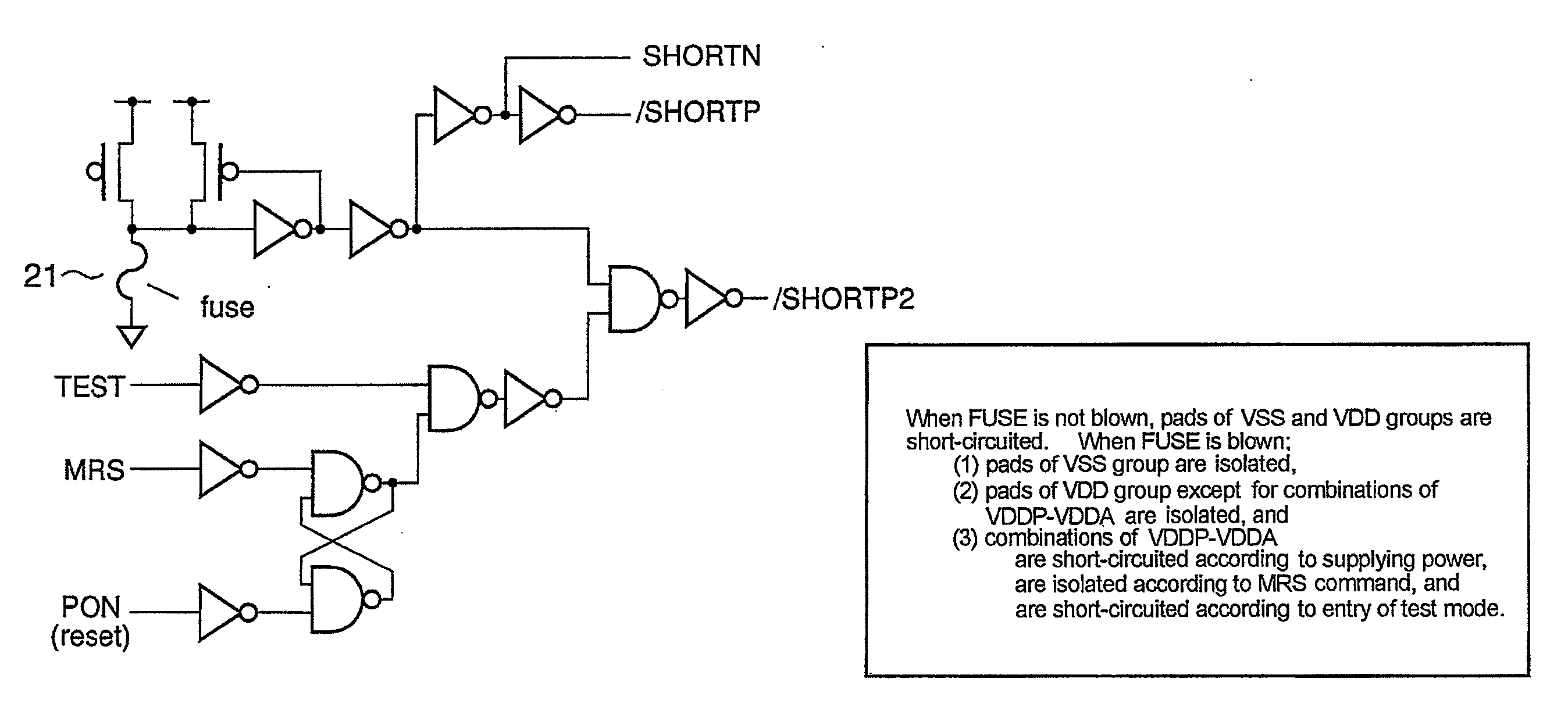
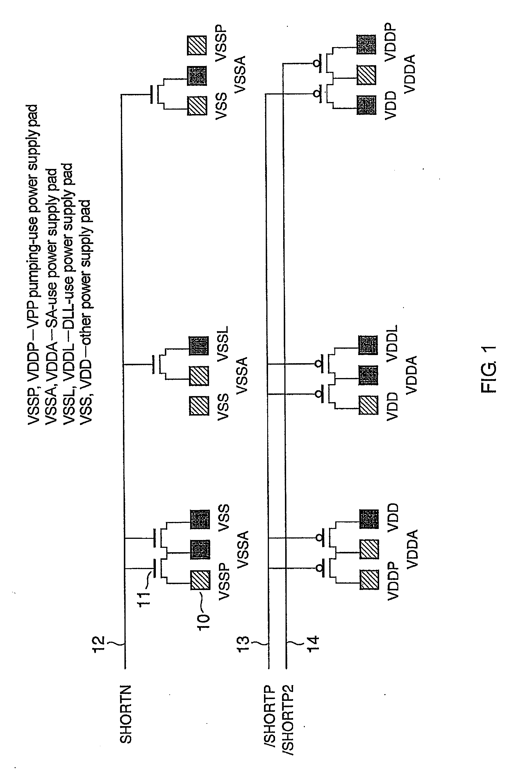
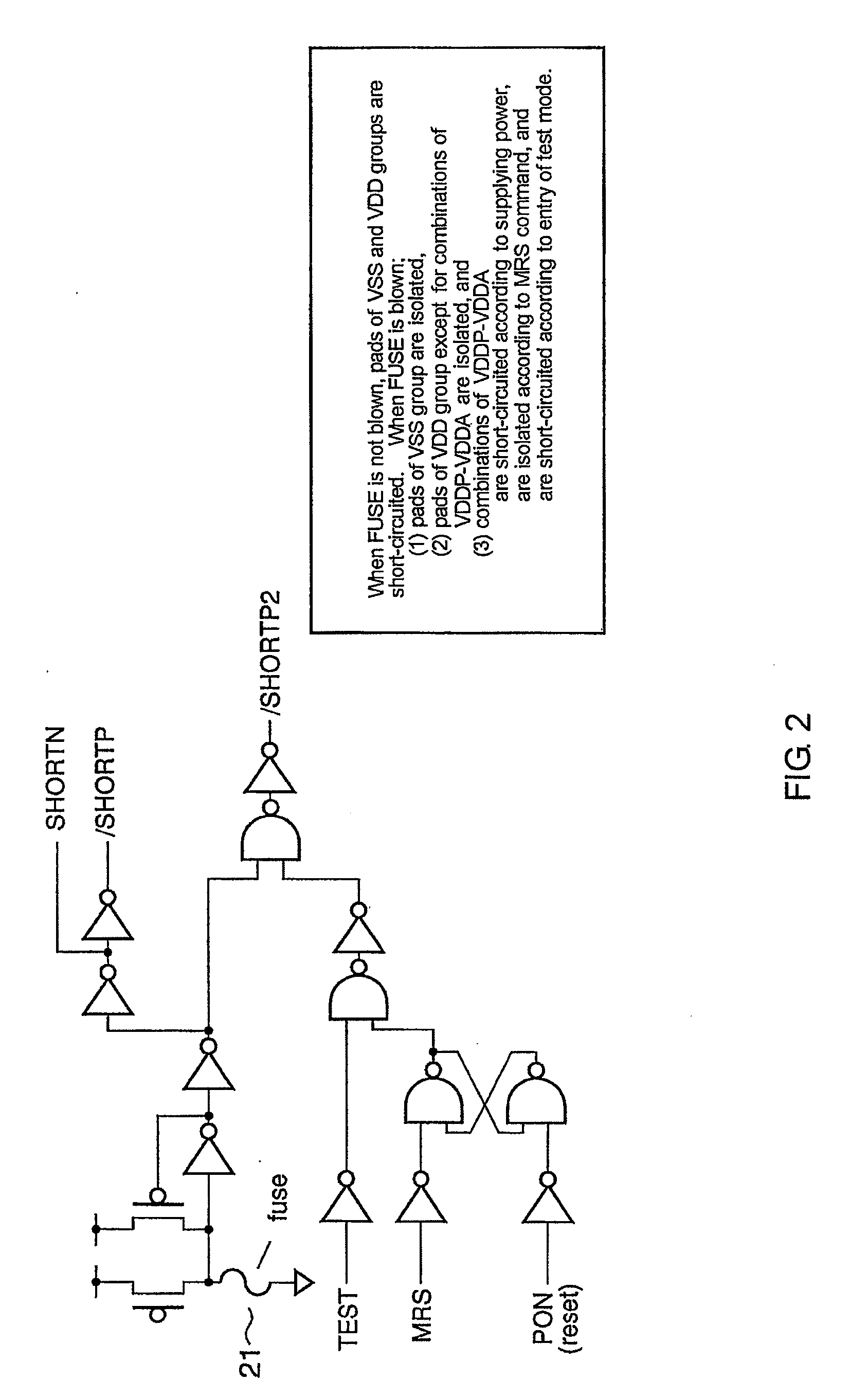
[0018]Referring now to FIG. 1, a semiconductor integrated circuit (or a chip) according to a first embodiment of the present invention includes a plurality of power supply pads 10. FIG. 1 shows an example of an arrangement of the power supply pads 10 depicted as small squares. The semiconductor integrated circuit further includes non-illustrated semiconductor devices. The semiconductor integrated circuit is, for example, a dynamic random access memory (DRAM).

[0019]In FIG. 1, the power supply pads 10 are classified into four kinds according to their intended use. That is, there are VPP pump-use power supply pads (VSSP and VDDP), SA-use power supply pads (VSSA and ...


PUM


Abstract

A semiconductor integrated circuit includes power supply pads of two or more kinds, switches each of which is connected between adjacent two of the power supply pads to allow short-circuiting them, and at least one control line connected to control terminals of the switches according to the kinds of the power supply pads connected to the switches.

Description

[0001]This application is based upon and claims the benefit of priority from Japanese Patent Application No. 2007-306789, filed on Nov. 28, 2007, the disclosure of which is incorporated herein in its entirety by reference.BACKGROUND OF THE INVENTION[0002]1. Field of the Invention[0003]This invention relates to a semiconductor integrated circuit.[0004]2. Description of Related Art[0005]In a manufacturing process of a related semiconductor integrated circuit, electric inspection called a probe test is executed for the semiconductor integrated circuit in a (wafer) state that the semiconductor integrated circuit is formed on a semiconductor substrate together with a lot of other semiconductor integrated circuits. The probe test is executed by making probes come in contact with pads formed on a wafer. To increase inspection efficiency by increasing the number of integrated circuits which are inspected at a time, it is necessary to reduce the number of probes which come in contact with th...

Claims


Application Information

Patent Timeline
Patent Type & Authority Applications(United States)
IPC IPC(8): G01R31/02G06F19/00G01R31/28H01L21/66H01L21/822H01L27/04
CPCG01R31/2884G01R31/3172G11C2029/5602G11C29/1201G11C29/48G01R31/31721
Inventor HIRANO, RYOSUZUKI, YUKIHIDEEGAWA, HIDEKAZU
Owner LONGITUDE SEMICON S A R L
Why Eureka
Try Eureka