
Method for producing polycrystalline silicon

a polycrystalline silicon and polycrystalline technology, applied in the direction of silicon compounds, sustainable manufacturing/processing, final product manufacturing, etc., can solve the problems of limited method electric power consumption rate and difficult further reduction of cost, and achieve high purity polycrystalline silicon and efficiently reduce chlorosilane

Inactive Publication Date: 2009-05-28
SUMITOMO CHEM CO LTD
View PDF6 Cites 5 Cited by
  • Summary
  • Abstract
  • Description
  • Claims
  • Application Information

AI Technical Summary

Benefits of technology

[0007]An objective of the present invention is to provide a method for producing high purity polycrystalline silicon by efficiently reducing chlorosilane with a metal.

Problems solved by technology

However, this method has a limit in electric power consumption rate, and it is hard to further decrease the cost.

Method used


Image

  • Method for producing polycrystalline silicon
  • Method for producing polycrystalline silicon
  • Method for producing polycrystalline silicon

Examples


example 1

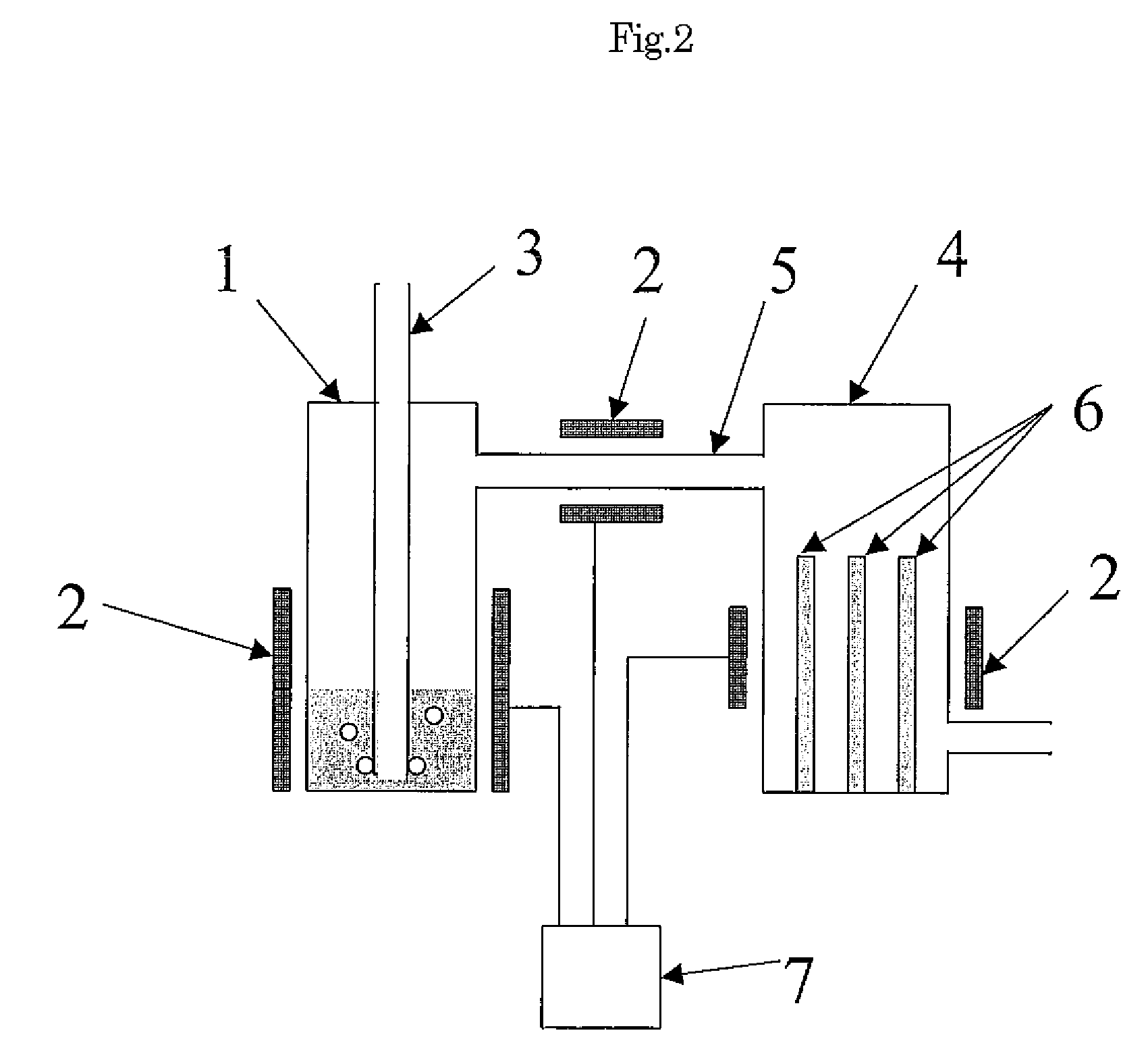
[0100]The apparatus shown in FIG. 7 was used.

[0101]An alumina protecting tube 14 (manufactured by NIKKATO CORPORATION, SSA-S, No. 8, inner diameter: 13 mm) including 10 g of aluminum (purity: 99.999% by weight, Fe: 0.73 ppm, Cu: 1.9 ppm, Ga: 0.57 ppm, Ti: 0.03 ppm, Ni: 0.02 ppm, Na: 0.02 ppm, Mg: 0.45 ppm, Zn: less than 0.05 ppm, B: 0.05 ppm, P: 0.27 ppm) was held in an alumina container 13, and was held in a vertical tubular furnace 11. Silicon tetrachloride gas (purity: 99.9999% by weight (6N), Fe: 5.2 ppb, Al: 0.8 ppb, Cu: 0.9 ppb, Mg: 0.8 ppb, Na: 2.4 ppb, Ca: 5.5 ppb, P: less than 1 ppm, B: less than 1 ppm, manufactured by Tri Chemical Laboratories Inc.) was introduced into molten aluminum for 4 hours at 1573K (1.68 times of the melting point of aluminum) and reacted. In order to carry out gas bubbling, the distance between a top end of a gas tube 12 (manufactured by NIKKATO CORPORATION, SSA-S, an outer diameter: 6 mm, inner diameter: 4 mm) and a bottom part of the alumina prot...

example 2

[0105]The aluminum protecting tube 14 having 11 g of aluminum was held in the alumina container 13, and held in the vertical tubular reactor 1. Then, silicon tetrachloride gas was introduced for 126 minutes into molten aluminum at 1573K and reacted at an atmospheric pressure.

[0106]Argon gas of 50 SCCM (flow rate: 50 mL / min., 0° C., 101.3 kPa) as a carrier gas was introduced into a container made of stainless steel in which silicon tetrachloride gas was filled. Vaporized gas was introduced into the reactor with the carrier gas. The feed rate of silicon tetrachloride per one minute was 0.44 g. The number of moles of the silicon tetrachloride was 0.69% with respect to the number of moles of aluminum. A flow rate of a gas component contacted with aluminum to have an equal temperature at the deposition zone was 3.58 m / min. The container made of stainless steel in which silicon tetrachloride was filled was held in the thermostatic vessel at 45° C. A vapor pressure of silicon tetrachloride...

example 3

[0107]Silicon tetrachloride gas was introduced into molten aluminum for 126 minutes at 1473K (1.58 times of the melting point of aluminum), and reacted. A gas flow rate at the deposition zone was 3.36 m / min. Except for this procedure the same procedures as Example 2 was repeated. The weight of silicon deposited on the wall of the alumina protecting tube was 1.2


PUM

PropertyMeasurementUnit
temperature T1aaaaaaaaaa
temperature T2aaaaaaaaaa
melting pointaaaaaaaaaa

Abstract

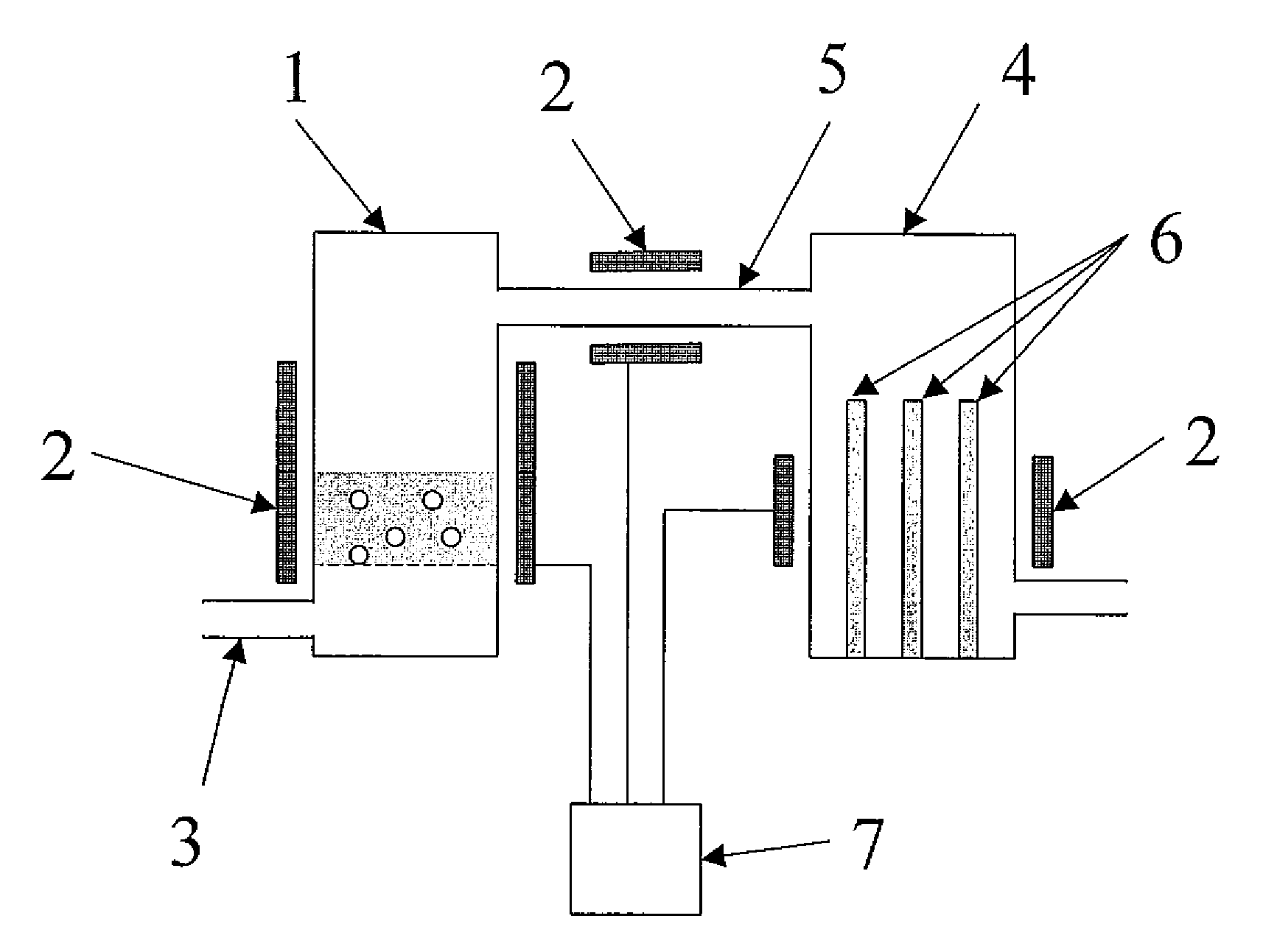
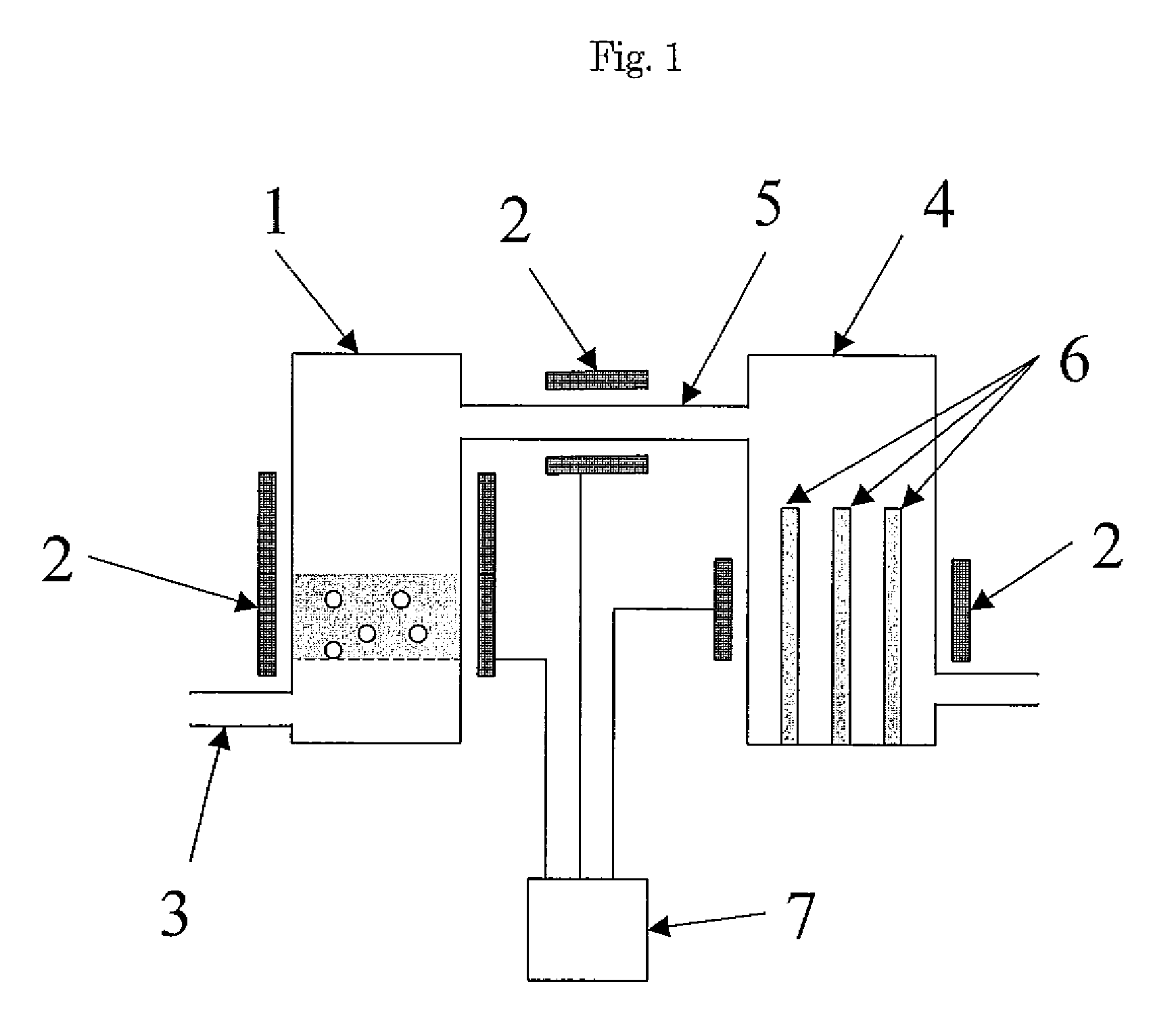
The present invention provides a method for producing polycrystalline silicon. The method for producing polycrystalline silicon comprises the steps of (A), (B), and (C),(A) reducing a chlorosilane represented by the formula (1) with a metal at a temperature Ti to obtain a silicon compound;SiHnCl4-n  (1)wherein n is an integer of 0 to 3,(B) transferring the silicon compound to a zone having a temperature T2, wherein T1>T2; and(C) depositing polycrystalline silicon in the zone having a temperature T2, wherein the temperature T1 is not less than 1.29 times of a melting point (Kelvin unit) of the metal, and the temperature T2 is higher than a sublimation point or boiling point of the chloride of the metal.

Description

TECHNICAL FIELD[0001]The present invention relates to a method for producing polycrystalline silicon.BACKGROUND ART[0002]An environmental problem has come to the fore and a solar cell is noted as a clean energy source. The demand of a solar cell is sharply increasing on residential purposes also in our country. A silicon-based solar cell is excellent in reliability and cell efficiency, and the silicon-based solar cell makes up about 80% of photovoltaic system. In order to increase the demand and decrease power generation cost, it is required to obtain a silicon material with low cost. At present as for a method for producing high purity silicon, most makers use Siemens method in which trichlorosilane is thermally decomposed. However, this method has a limit in electric power consumption rate, and it is hard to further decrease the cost.[0003]As a method instead of a thermal decomposition, a method of reducing chlorosilane using zinc or aluminum to obtain silicon is proposed. For exa...

Claims


Application Information

Patent Timeline
Patent Type & Authority Applications(United States)
IPC IPC(8): C01B33/03B01J19/00
CPCC01B33/033Y02E10/546H01L31/182Y02P70/50
Inventor YAMABAYASHI, TOSHIHARUHATA, MASAHIKO
Owner SUMITOMO CHEM CO LTD
Learn More