
Ag-based sputtering target

a technology of sputtering target and sputtering medium, which is applied in the direction of electrolysis components, vacuum evaporation coatings, coatings, etc., can solve the problems of not meeting the required properties and the average grain size of the target exceeds 15 m, and achieves uniform film thickness and small grain size variations.

Inactive Publication Date: 2009-06-04
KOBELCO RES INST
View PDF45 Cites 15 Cited by
  • Summary
  • Abstract
  • Description
  • Claims
  • Application Information

AI Technical Summary

Benefits of technology

[0028]If the Ag-based sputtering target in accordance with the aspect of the present invention is used, an Ag-based thin film with extremely uniform film thickness (and also componential composition, in the case of Ag alloy) in the film plane direction can be formed. Accordingly, the Ag-based sputtering target in accordance with the present invention is particularly suitably used for forming the Ag-based thin film used for the usage of the technical field, particularly, of very thin film thickness of approximately 20-200 Å (=2-20 nm), for example, a semi-transparent reflective film of the present generation and next generation optical disks, a low-E film for a heat ray reflective / cutoff window glass, and a shield film for an electromagnetic wave shield.

Problems solved by technology

However, in all of the sputtering targets described in the patent documents 1-5, the average grain sizes of the targets exceed 15 μm which cannot satisfy the required properties described above.

Method used


Image

  • Ag-based sputtering target
  • Ag-based sputtering target
  • Ag-based sputtering target

Examples


example

[0091]Although the present invention will be described below further specifically by referring to the examples, the present invention intrinsically is by no means to be limited by the examples below and can of course be implemented with appropriate modifications added within the scope adaptable to the purposes described above and below, and any of them is to be included within the technical range of the present invention.

(1) Manufacturing of the Sputtering Target

[0092]On the basis of the manufacturing condition in accordance with the present invention, Ag alloy sputtering targets (examples of the present invention) of the sample Nos. 1-5 shown in Table 2 were manufactured. Specifically, the Ag alloy sputtering targets of the examples of the present invention were manufactured by; using Ag alloys (name: a-f) of a variety of kinds of composition shown in Table 1, and performing the SF process and the HIP process as shown in Table 2 and the plastic working process (working temperature ...


PUM

PropertyMeasurementUnit
Grain sizeaaaaaaaaaa
Lengthaaaaaaaaaa
Fractionaaaaaaaaaa

Abstract

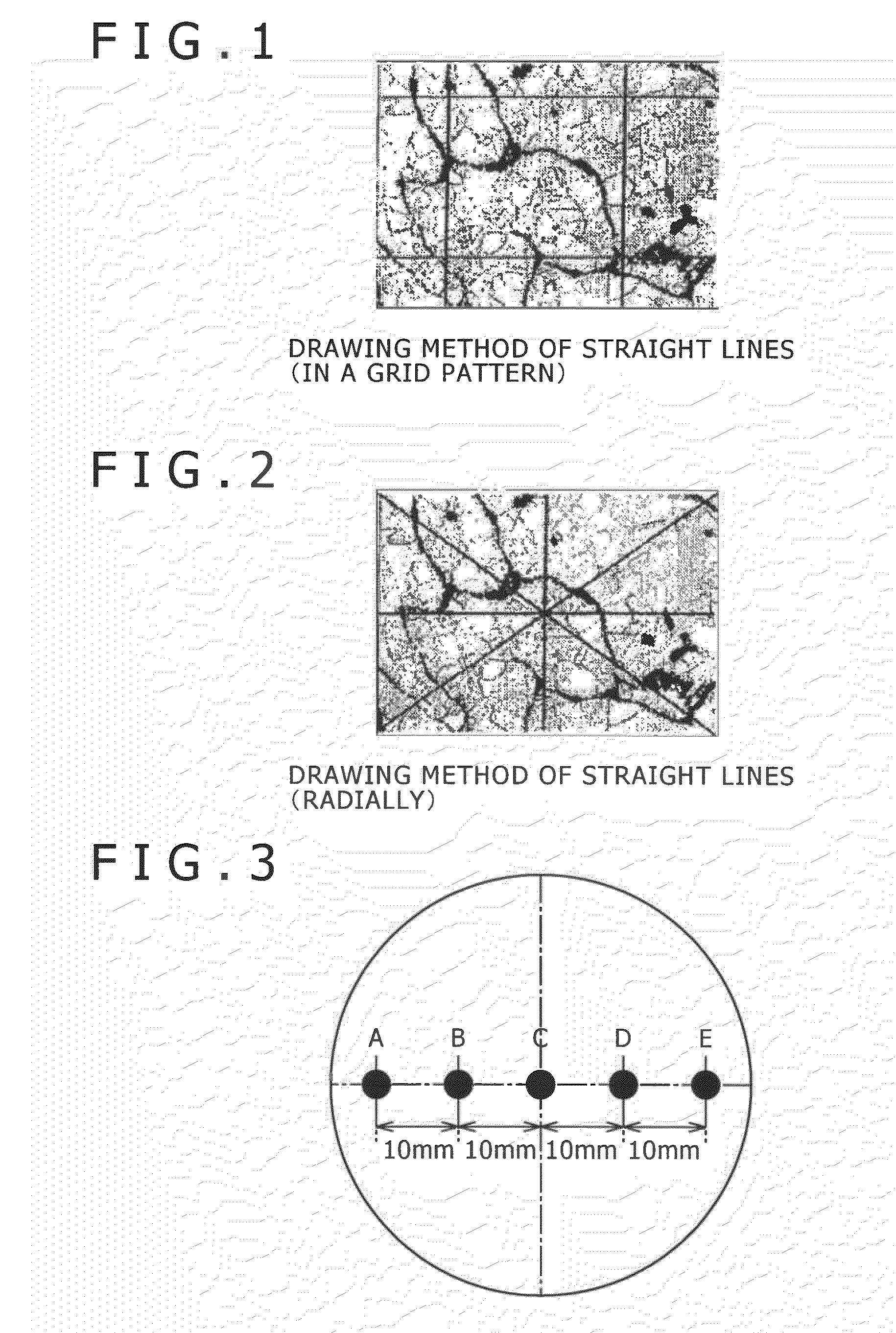
Disclosed is an Ag-based sputtering target composed of pure Ag or Ag alloy wherein when the average grain size dave of the sputtering face of the Ag-based sputtering target is measured in accordance with the procedures 1-3 described below, the average grain size dave satisfies 10 μm or less.(Procedure 1) In the surface of the sputtering face, a plurality of locations are optionally selected, and a micrograph (magnification: 40-2,000 times) of each selected location is taken.(Procedure 2) Four or more straight lines are drawn in a grid pattern or radially on each micrograph, a number n of grain boundaries existing on the straight line is investigated, and a grain size d is calculated on the basis of the following equation on each straight line.d=L / n / m where, L represents the length of the straight line, n represents the number of the grain boundaries existing on the straight line, and m represents the magnification of the micrograph.(Procedure 3) The average value of the grain sizes d of all selected locations is made the average grain size dave of the sputtering face.

Description

BACKGROUND OF THE INVENTION[0001]1. Field of the Invention[0002]The present invention relates to an Ag-based sputtering target useful for forming an Ag-based thin film by a sputtering method and an Ag-based thin film obtainable using the Ag-based sputtering target, more specifically relates to an Ag-based sputtering target capable of forming an Ag-based thin film extremely excellent in in-plane uniformity.[0003]2. Description of the Related Art[0004]The Ag-based thin film of pure Ag or Ag alloy and the like is excellent in optical properties such as high reflectance and transmittance and a low extinction coefficient, excellent in thermal properties with high thermal conductivity, and excellent in electrical properties with low electrical resistivity, and has excellent surface smoothness. Therefore, the Ag-based thin film is widely applied, for example, to; a reflective film, a semi-transparent reflective film, and a thermal diffusion film for an optical information record medium (op...

Claims


Application Information

Patent Timeline
IPC IPC(8): C23C14/34
CPCC22C5/06C23C14/3414C22F1/14C22C5/08
Inventor MATSUZAKI, HITOSHI
Owner KOBELCO RES INST
Learn More