Thin film transistor, display device having thin film transistor, and method for manufacturing the same

a technology of thin film transistor and display device, which is applied in the direction of transistors, semiconductor devices, electrical devices, etc., can solve the problems of reducing yield, increasing cost, and requiring a more complicated process, and achieves low cost, high current, and high mobility.

Inactive Publication Date: 2009-06-04
SEMICON ENERGY LAB CO LTD
View PDF60 Cites 38 Cited by
  • Summary
  • Abstract
  • Description
  • Claims
  • Application Information

AI Technical Summary

Benefits of technology

[0028]According to the present invention, by using a semiconductor film that mainly contains germanium for a channel formation region, a thin film transistor with high mobility and high on current can be manufactured. In addition, by providing a buffer layer between the semiconductor film that mainly contains germanium and serves as a channel formation region, and source and drain regions, a thin film transistor with low off current can be manufactured. In other words, a thin film transistor with excellent electric characteristics can be manufactured. Further, a display device having the thin film transistor can be manufactured.

Problems solved by technology

However, the thin film transistor in which a polycrystalline semiconductor film is used for a channel formation region requires a more complicated process than the thin film transistor in which an amorphous semiconductor film is used for a channel formation region because of crystallization of the semiconductor film.
Thus, there are problems such as a reduction in yield and an increase in cost.
A thin film transistor in which a microcrystalline germanium film is used for a channel formation region has a problem of high off current.
Further, a thin germanium film has a problem in that it has low adhesiveness on an insulating film and a manufacturing yield of thin film transistors having the thin germanium film is low.

Method used


Image

  • Thin film transistor, display device having thin film transistor, and method for manufacturing the same
  • Thin film transistor, display device having thin film transistor, and method for manufacturing the same
  • Thin film transistor, display device having thin film transistor, and method for manufacturing the same

Examples


embodiment mode 1

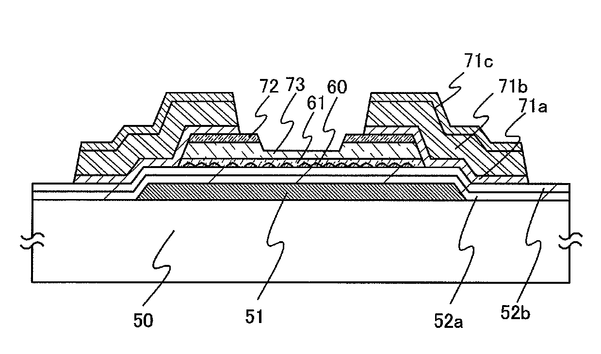
[0061]In a thin film transistor illustrated in FIG. 1, a gate electrode 51 is formed over a substrate 50; gate insulating films 52a and 52b are formed over the gate electrode 51; crystal grains 60 that mainly contain silicon are formed over the gate insulating films 52a and 52b; a semiconductor film 61 that mainly contains germanium is formed over the crystal grains 60 that mainly contain silicon and over the gate insulating film 52b; a buffer layer 73 is formed over the semiconductor film 61 that mainly contains germanium; a pair of semiconductor films 72 to which an impurity element imparting one conductivity type is added are formed over the buffer layer 73; and wirings 71a to 71c are formed over the pair of semiconductor films 72 to which the impurity element imparting one conductivity type is added. Carriers travel through the semiconductor film 61 that mainly contains germanium because the semiconductor film 61 that mainly contains germanium has higher mobility than the crysta...

embodiment mode 2

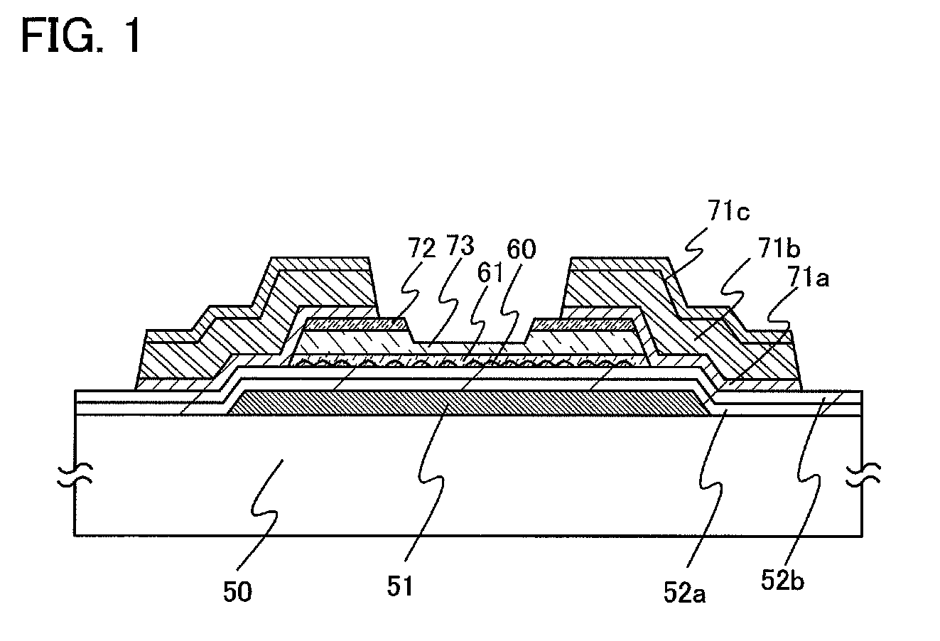
[0081]This embodiment mode presents a thin film transistor which includes a semiconductor film that mainly contains germanium, has higher mobility, and can improve a yield compared to that in Embodiment Mode 1, with reference to FIG. 2.

[0082]In the thin film transistor illustrated in FIG. 2, a gate electrode 51 is formed over a substrate 50; gate insulating films 52a and 52b are formed over the gate electrode 51; crystal grains 68 that mainly contain silicon and include a donor impurity element are formed over the gate insulating films 52a and 52b; a semiconductor film 61 that mainly contains germanium is formed over the crystal grains 68 that mainly contain silicon and include the donor impurity element, and over the gate insulating film 52b; a buffer layer 73 is formed over the semiconductor film 61 that mainly contains germanium; a pair of semiconductor films 72 to which an impurity element imparting one conductivity type is added are formed over the buffer layer 73; and wirings ...

embodiment mode 3

[0088]This embodiment mode presents a thin film transistor which includes a semiconductor film that mainly contains germanium, has higher mobility, and can improve a yield compared to that in Embodiment Mode 1, with reference to FIG. 3.

[0089]In the thin film transistor illustrated in FIG. 3, a gate electrode 51 is formed over a substrate 50; a gate insulating film 52a is formed over the gate electrode 51; a gate insulating film 41 having an uneven surface is formed over the gate insulating film 52a; crystal grains 60 that mainly contain silicon are formed over the gate insulating film 41; a semiconductor film 61 that mainly contains germanium is formed over the crystal grains 60 that mainly contain silicon and over the gate insulating film 41; a buffer layer 73 is formed over the semiconductor film 61 that mainly contains germanium; a pair of semiconductor films 72 to which an impurity element imparting one conductivity type is added are formed over the buffer layer 73; and wirings ...


PUM


Abstract

A thin film transistor with excellent electric characteristics, a display device having the thin film transistor, and a method for manufacturing the thin film transistor and the display device in a high yield are provided. In the thin film transistor, a gate electrode, a gate insulating film, crystal grains that mainly contain silicon and are provided for a surface of the gate insulating film, a semiconductor film that mainly contains germanium and covers the crystal grains and the gate insulating film, and a buffer layer in contact with the semiconductor film that mainly contains germanium overlap with one another. Further, the display device has the thin film transistor.

Description

BACKGROUND OF THE INVENTION[0001]1. Field of the Invention[0002]The present invention relates to a thin film transistor, a display device having the thin film transistor at least in a pixel portion, and methods for manufacturing the same.[0003]2. Description of the Related Art[0004]In recent years, technology for forming thin film transistors (TFTs) using a thin semiconductor film (with a thickness of from several tens of nanometers to several hundreds of nanometers, approximately) formed over a substrate having an insulating surface has been attracting attention. Thin film transistors are applied to a wide range of electronic devices such as ICs or electrooptic devices, and prompt development of thin film transistors that are to be used as switching elements in image display devices, in particular, is being pushed.[0005]As a switching element in an image display device, a thin film transistor including an amorphous semiconductor film, a thin film transistor including a polycrystall...

Claims


Application Information

Patent Timeline
Patent Type & Authority Applications(United States)
IPC IPC(8): H01L29/786H01L21/336
CPCH01L21/02532H01L21/0262H01L21/67017H01L21/67207H01L27/1214H01L29/78696H01L29/41733H01L29/4908H01L29/66742H01L29/78687H01L29/04H01L27/1248H01L27/1288
Inventor YAMAZAKI, SHUNPEI
Owner SEMICON ENERGY LAB CO LTD
Why Eureka
Try Eureka