Semiconductor device and manufacturing method of the same

a technology of mosfet and semiconductors, which is applied in the direction of mosfets, basic electric elements, electrical appliances, etc., can solve the problems of unsuitable manpower for mosfets, and achieve the effects of scaling down, increasing the concentration of impurity layers, and low on-resistan

Inactive Publication Date: 2009-06-04
RENESAS ELECTRONICS CORP
View PDF2 Cites 156 Cited by
  • Summary
  • Abstract
  • Description
  • Claims
  • Application Information

AI Technical Summary

Benefits of technology

[0011]That is, the typical one is characterized by forming a trench-shaped source electrode (a source trench) in order to increase the impurity concentration of a drift layer while maintaining the drain-source breakdown voltage. More specifically, with the RESURFE effect by the source trench, the drain-source breakdown voltage is maintained even if the impurity concentration in the drift layer is increased, whereby the power MOSFET with the low on-resistance can be provided. Besides, since a body contact is made in the source trench, there is no need to provide a region for the body contact in other region of the front surface of the semiconductor device, and further scaling-down can be achieved.

Problems solved by technology

However, since an impurity implanted deeply in order to form the column region described above is diffused in a horizontal direction in the manufacturing method according to Patent document 1 described above, there is a problem that this manner is inappropriate for the power MOSFET with low breakdown voltage having a fine structure.

Method used


Image

  • Semiconductor device and manufacturing method of the same
  • Semiconductor device and manufacturing method of the same
  • Semiconductor device and manufacturing method of the same

Examples


first embodiment

[0041]The semiconductor device according to a first embodiment of the present invention is described with reference to FIG. 1 to FIG. 5.

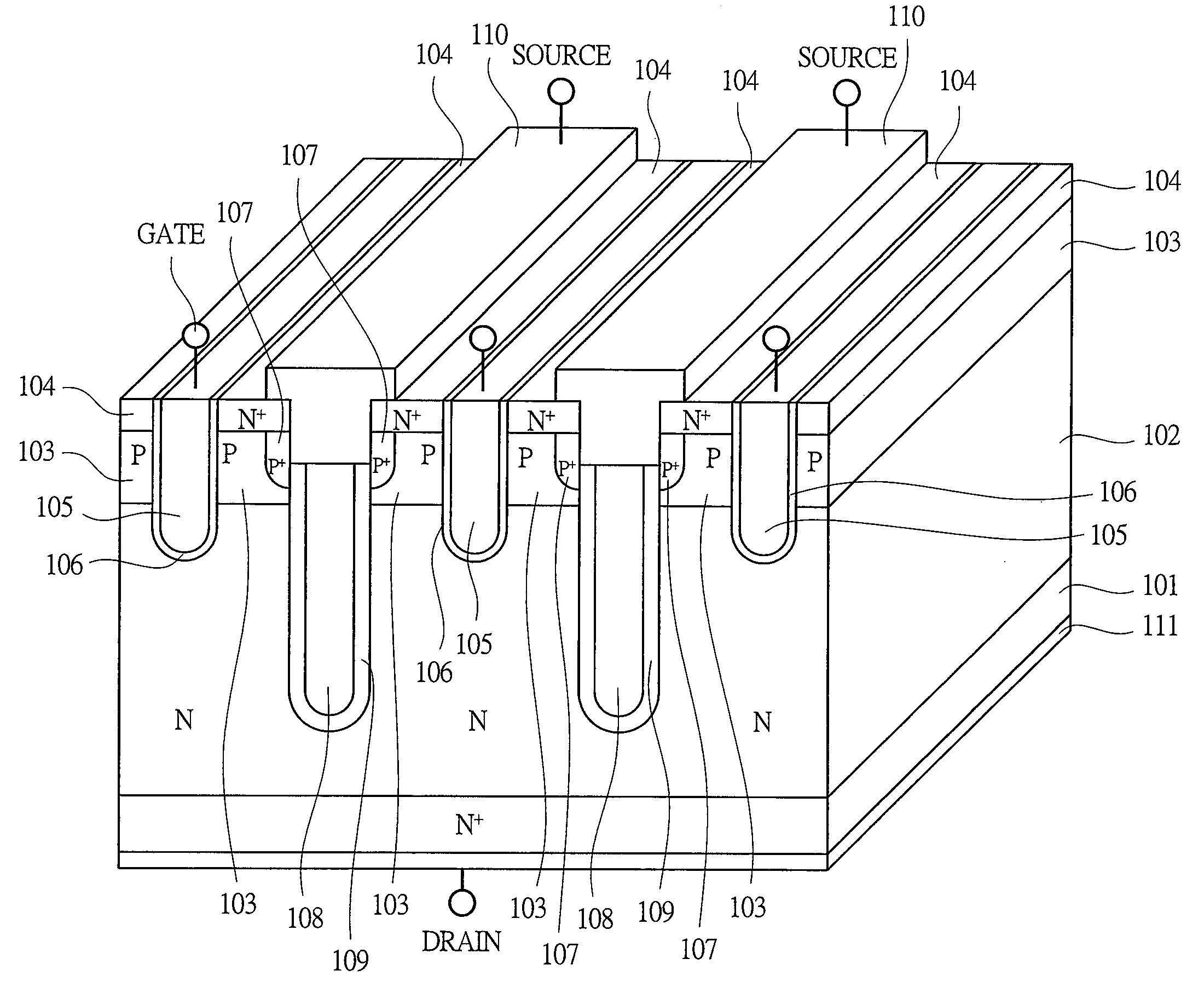
[0042]FIG. 1 shows an example of a structure of a vertical trench MOSFET with low breakdown voltage having a RESURF structure according to the first embodiment of the present invention.

[0043]In the vertical trench MOSFET according to the first embodiment, an N type epitaxial region 102, a channel region 103, a source region 104, a gate electrode 105, a gate insulator 106, a body contact region 107, a trench-buried source electrode 108, a trench-buried source insulator 109, and the like are formed on an N+ type substrate 101, and a source electrode 110 is formed on the front surface thereof and a drain electrode 111 is formed on the rear surface thereof.

[0044]More particularly, the N type epitaxial region 102 formed on the upper surface of the N+ type substrate 101 having the drain electrode 111 on the lower surface thereof, a gate trench extending f...

second embodiment

[0061]A semiconductor device according to a second embodiment of the present invention is described with reference to FIG. 6 and FIG. 7.

[0062]FIG. 6 shows an example of a structure of the vertical trench MOSFET with low breakdown voltage having the RESURF structure according to the second embodiment of the present invention.

[0063]The vertical trench MOSFET according to the second embodiment is different from the first embodiment in the following points. The present embodiment is characterized in that the distance from the front surface to the bottom of the gate trench is equal to the distance from the front surface to the bottom of the field trench, the gate insulator of the bottom surface in the gate trench is thicker than that of the side surface in the gate trench, and the process of forming the gate trench and the process of forming the field trench are performed at the same time. Also, the present embodiment is characterized in that a thickness of a gate insulator 201 of the bo...

third embodiment

[0070]A semiconductor device according to a third embodiment of the present invention is described with reference to FIG. 8.

[0071]FIG. 8 shows an example of a structure of the vertical trench MOSFET with low breakdown voltage having the RESURF structure according to the third embodiment of the present invention.

[0072]The vertical trench MOSFET according to the third embodiment is different from the first embodiment in the following point. The present embodiment is characterized in that a more highly-doped body contact region 302 than the channel region 103 is selectively formed on the front surface of the channel region 103.

[0073]More specifically, in the vertical trench MOSFET according to the present embodiment, on the front surface of the channel region 103, the body contact region 302 is formed so as to be alternately disposed with the source region 301 in a backward direction. In this manner, in addition to the effect of the first embodiment, the sufficient avalanche resistance...


PUM


Abstract

The vertical trench MOSFET comprises: an N type epitaxial region formed on an upper surface of an N+ type substrate having a drain electrode on a lower surface thereof; a gate trench extending from a front surface into the N type epitaxial region; a gate electrode positioned in the gate trench so as to interpose an insulator; a channel region formed on the N type epitaxial region; a source region formed on the channel region; a source electrode formed on the source region; a source trench extending from the front surface into the N type epitaxial region; and a trench-buried source electrode positioned in the source trench so as to interpose an insulator, wherein the source electrode contacts with the trench-buried source electrode.

Description

CROSS-REFERENCE TO RELATED APPLICATION[0001]The present application claims priority from Japanese Patent Application No. JP 2007-312001 filed on Dec. 3, 2007, the content of which is hereby incorporated by reference into this application.TECHNICAL FIELD OF THE INVENTION[0002]The present invention relates to a semiconductor device of a power MOSFET (Metal Oxide Semiconductor-Field Effect Transistor). More particularly, it relates to a technology effectively applied to a device structure to realize the low on-resistance in a power MOSFET with low breakdown voltage and a manufacturing method thereof.BACKGROUND OF THE INVENTION[0003]According to a consideration of the present inventors, in a power supply of information equipment and the like, a further reduction in loss is required from the viewpoint of power consumption and thermal design. In particular, in a power MOSFET with low breakdown voltage (for example, breakdown voltage of 30 V) used therein, the reduction in on-resistance is...

Claims


Application Information

Patent Timeline
Patent Type & Authority Applications(United States)
IPC IPC(8): H01L29/78H01L21/336H01L29/06
CPCH01L29/0696H01L29/0878H01L29/1095H01L29/407H01L29/7813H01L29/42368H01L29/66727H01L29/66734H01L29/7802H01L29/41741
Inventor HIRAO, TAKASHIHASHIMOTO, TAKAYUKIAKIYAMA, NOBORU
Owner RENESAS ELECTRONICS CORP
Why Eureka
Try Eureka