Flip chip package and method for manufacturing the same
- Summary
- Abstract
- Description
- Claims
- Application Information
AI Technical Summary
Benefits of technology
Problems solved by technology
Method used
Image

Examples
Embodiment Construction
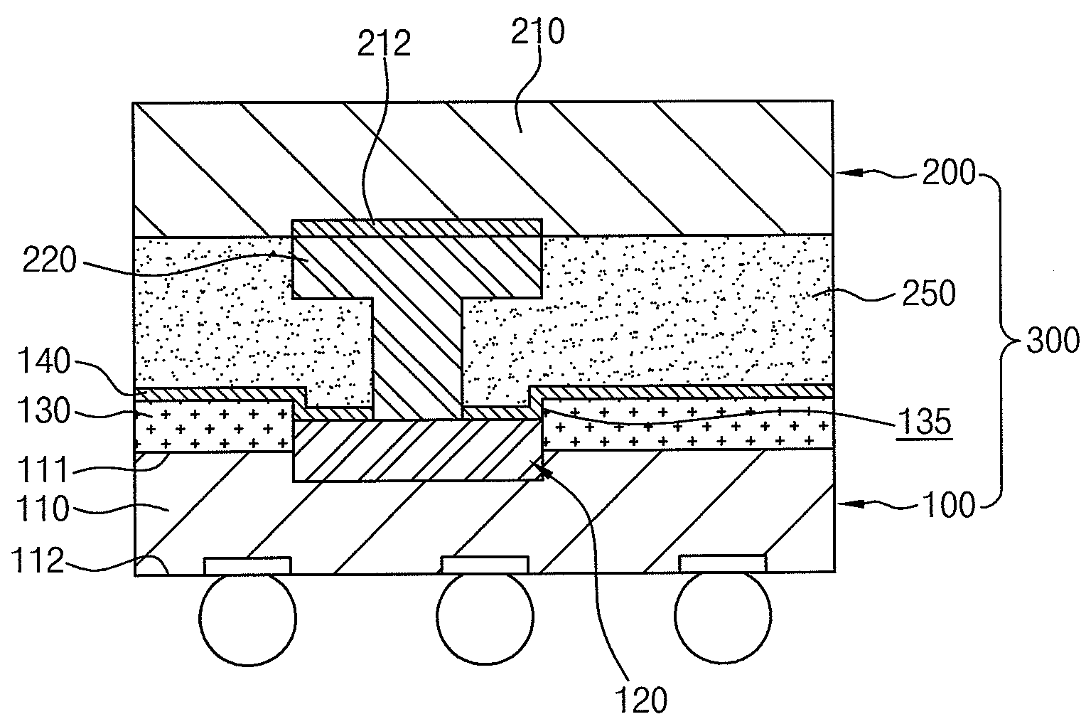
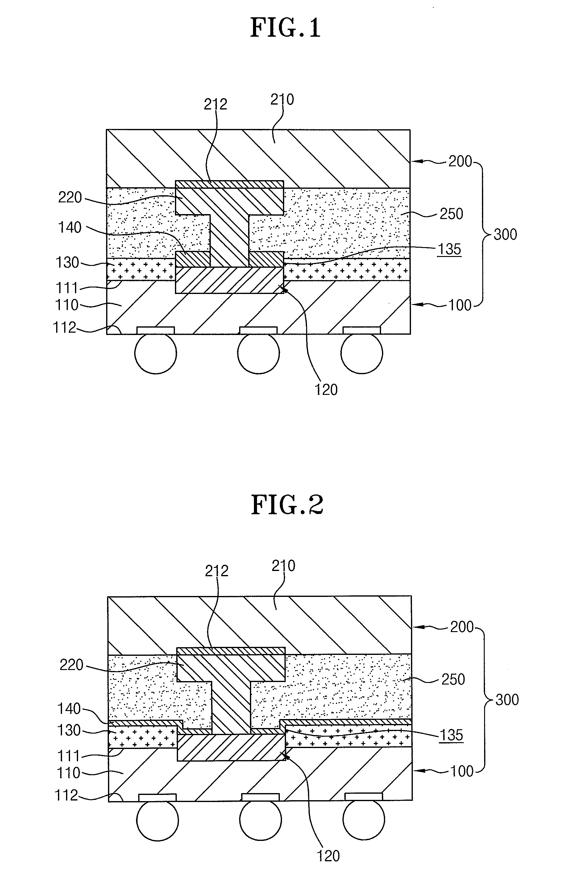
[0040]FIG. 1 is a cross-sectional view illustrating a flip chip package in accordance with an embodiment of the present invention.
[0041]A flip chip package 300 includes a substrate 100 and a semiconductor chip 200.
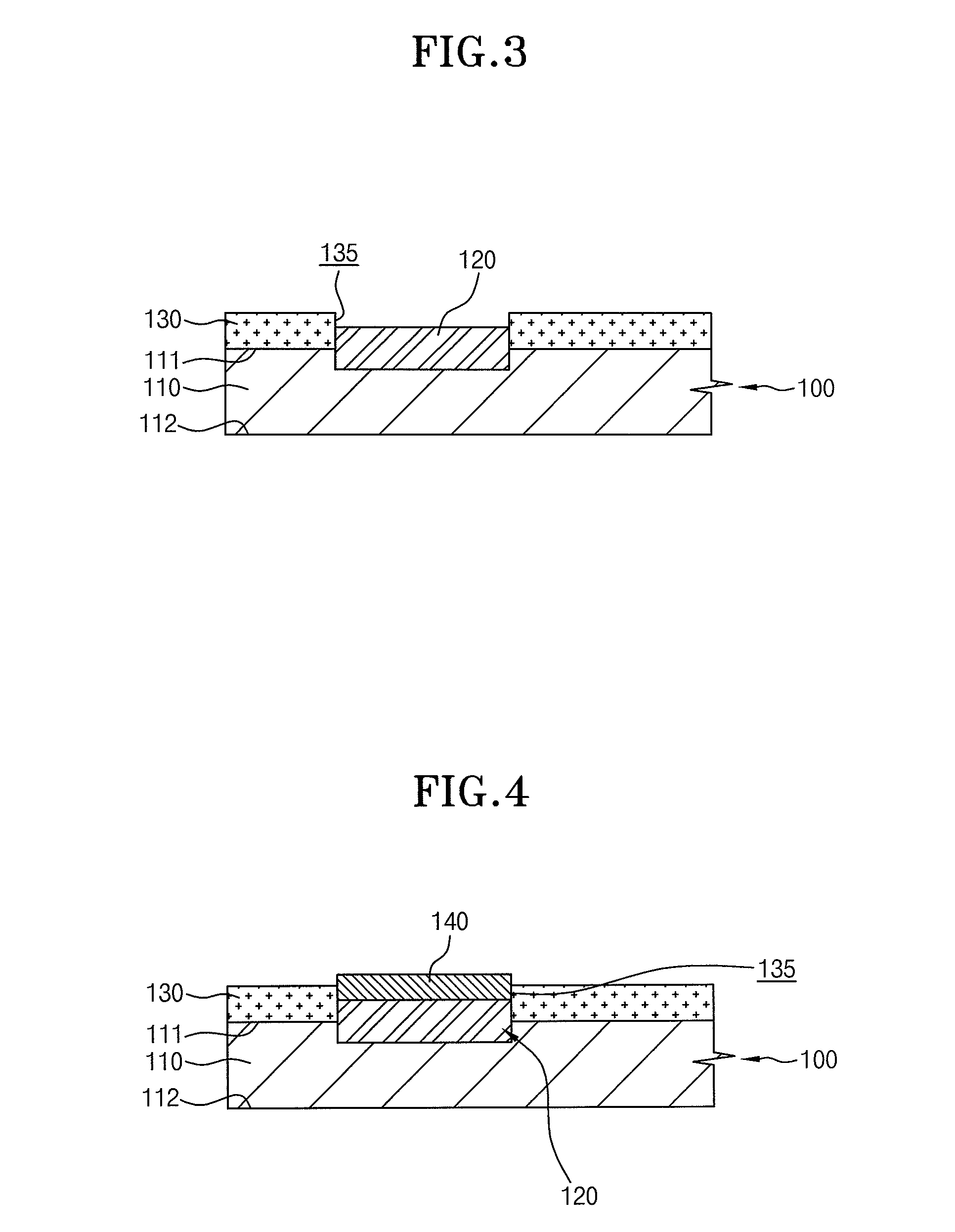
[0042]The semiconductor chip 100 includes a substrate body 110, a terminal part 120 of a metal wiring, a solder resist pattern 130, and an organic anti-oxidation layer 140.
[0043]The substrate body 110 is, for example, a plate shaped printed circuit board (PCB). The substrate body 110 includes a first surface 111 and a second surface 112 opposite to the first surface 111.
[0044]The terminal part 120 of the metal wiring is disposed, for example, over the first surface 111 of the substrate body 110. In the present embodiment, the terminal part 120 of the metal wiring may include, for example, copper having superior electrical characteristics.
[0045]The solder resist pattern 130 is disposed over the first surface 111 of the substrate body 110. The solder resist pattern 130 has a...
PUM
| Property | Measurement | Unit |
|---|---|---|
| Temperature | aaaaa | aaaaa |
| Temperature | aaaaa | aaaaa |
| Temperature | aaaaa | aaaaa |
Abstract
Description
Claims
Application Information
 - R&D
- Intellectual Property
- Life Sciences
- Materials
- Tech Scout
- Unparalleled Data Quality
- Higher Quality Content
- 60% Fewer Hallucinations
Browse by: Latest US Patents, China's latest patents, Technical Efficacy Thesaurus, Application Domain, Technology Topic, Popular Technical Reports.
© 2025 PatSnap. All rights reserved.Legal|Privacy policy|Modern Slavery Act Transparency Statement|Sitemap|About US| Contact US: help@patsnap.com