Semiconductor integrated circuit

a technology of integrated circuits and semiconductors, applied in the field of semiconductor integrated circuits, can solve problems such as the inability to realize patent documents 2 and 3 like the sample and hold circuit of the first forma

Active Publication Date: 2009-06-04
RENESAS ELECTRONICS CORP
View PDF10 Cites 31 Cited by
  • Summary
  • Abstract
  • Description
  • Claims
  • Application Information

AI Technical Summary

Benefits of technology

[0025]Further, the cyclic A / D converter described in the patent document 2 can reduce the influence on an A / D conversion result of the offset voltage of the internal amplifier by switching between the cross-couple connection and the straight connection of two feedback capacitors between the differential input and the differential output of the amplifier. However, the cyclic A / D converter is an extremely special A / D converter, so that it cannot be applied to the successive-approximation-type A / D converter as described in the patent document 1.
[0044]In the latter half of the sampling period of the analog input terminal AN0 of the zero channel, the first switch SW01 is controlled to the off state and, after that, the second switch SW02 is controlled to the on state. Therefore, the analog input signal voltage of the analog input terminal AN0 of the zero channel in the multiplexer MPX is output to the analog output terminal ADCOM of the multiplexer MPX via the second switch SW02 while bypassing the voltage follower configured by the operational amplifier OpAmp0 and the first switch SW01. As a result, even if the input offset voltage exists between the non-inverting input terminal + and the inverting input terminal − of the operational amplifier OpAmp0 of the voltage follower, by the bypass function of the second switch SW02, the influence of the input offset voltage to the voltage level of the analog output terminal ADCOM can be reduced.
[0051]Therefore, an object of the present invention is to reduce offset error voltage at signal source impedance in analog input signal voltage supplied to an input terminal due to input offset voltage of an operational amplifier as a component of a sapling circuit or a multiplexer coupled to an input terminal of an A / D converter.
[0058]As a result, the polarity of the sampling error voltage at the signal source impedance of the analog input terminal of the sampling circuit due to the input offset voltage between the first and second input terminals of the operational amplifier changes between the first and second sample modes. Therefore, the average voltage level obtained by time integration of the sampling error voltage whose polarity changes becomes almost zero, so that the offset error voltage at the signal source impedance can be reduced.

Problems solved by technology

However, in the switched-capacitor-type sample and hold circuit of the second format, operations similar to those of the hold and voltage comparison mode of the switched-capacitor-type comparator described in the non-patent document 3 like the sample and hold circuit of the first format described in the non-patent document 2 cannot be realized.

Method used


Image

  • Semiconductor integrated circuit
  • Semiconductor integrated circuit
  • Semiconductor integrated circuit

Examples


Embodiment Construction

Representative Embodiments

[0080]First, outline of representative embodiments of the present invention disclosed in the application will be described. Reference numerals in the diagrams referred to in the description of the outline in parenthesis with respect to the representative embodiments simply denote concept of components.

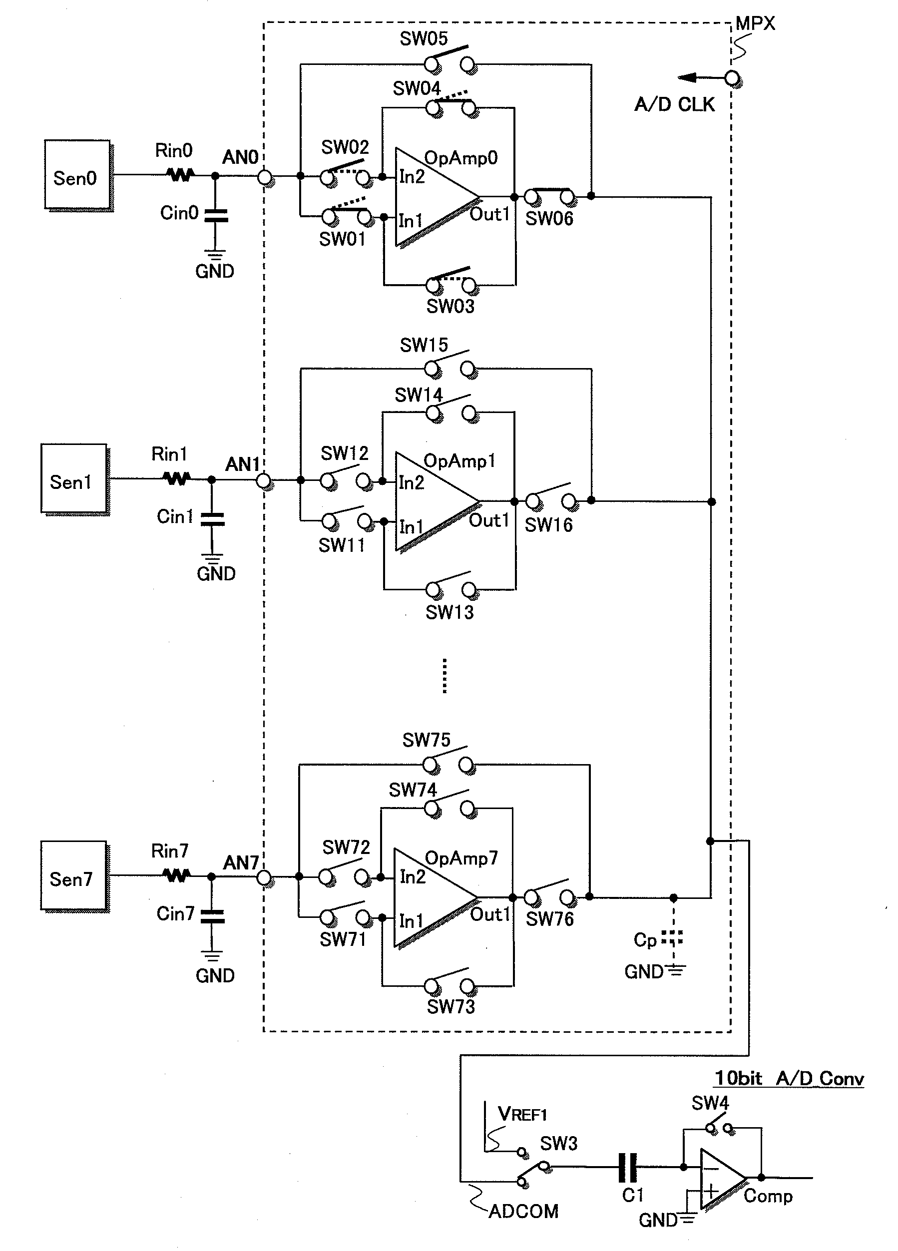
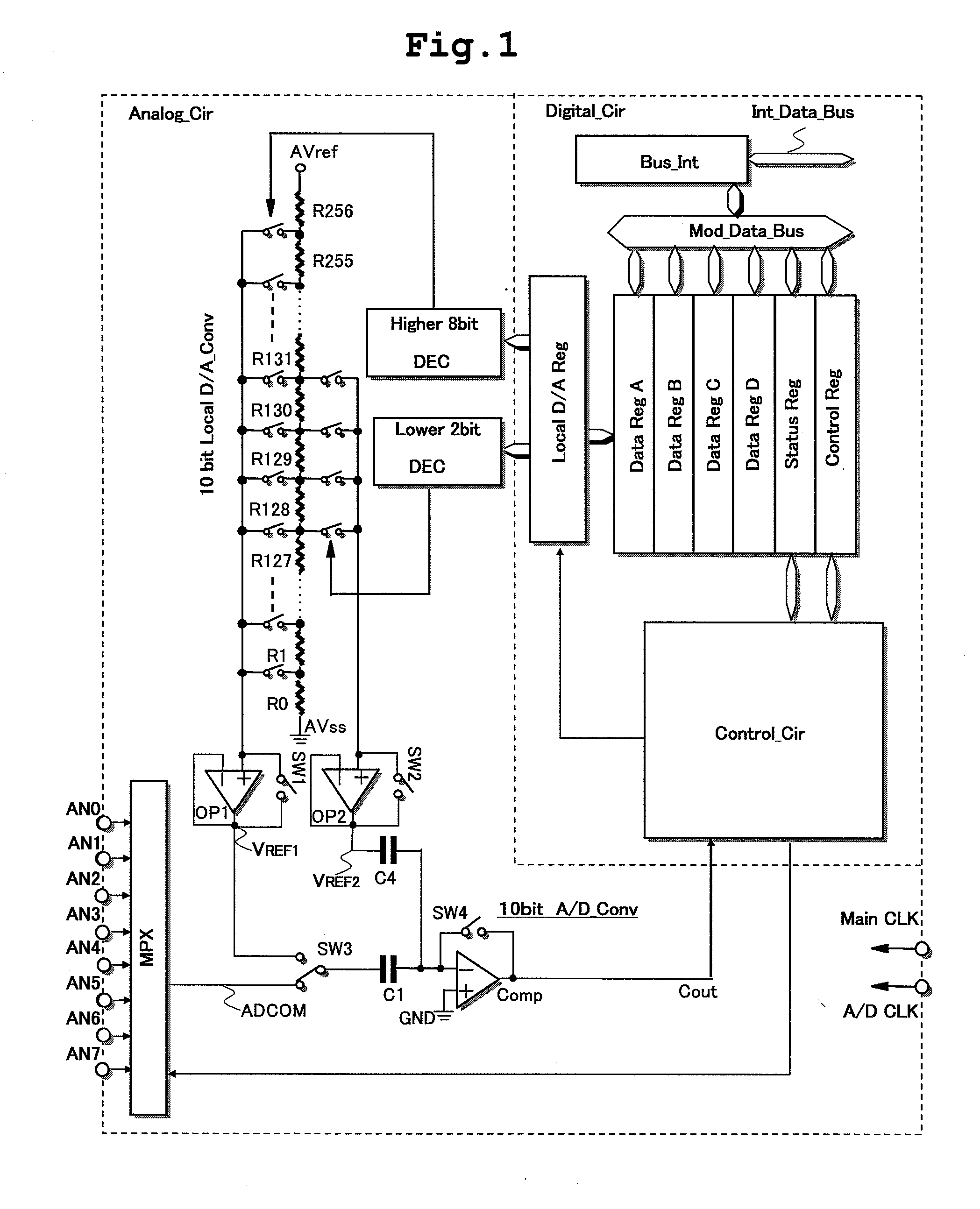
[0081][1]. A semiconductor integrated circuit as a representative embodiment of the present invention has an A / D converter (10-bit A / D_Conv) and a sampling circuit (MPX) coupled to an input terminal of the A / D converter (refer to FIGS. 1 and 5).

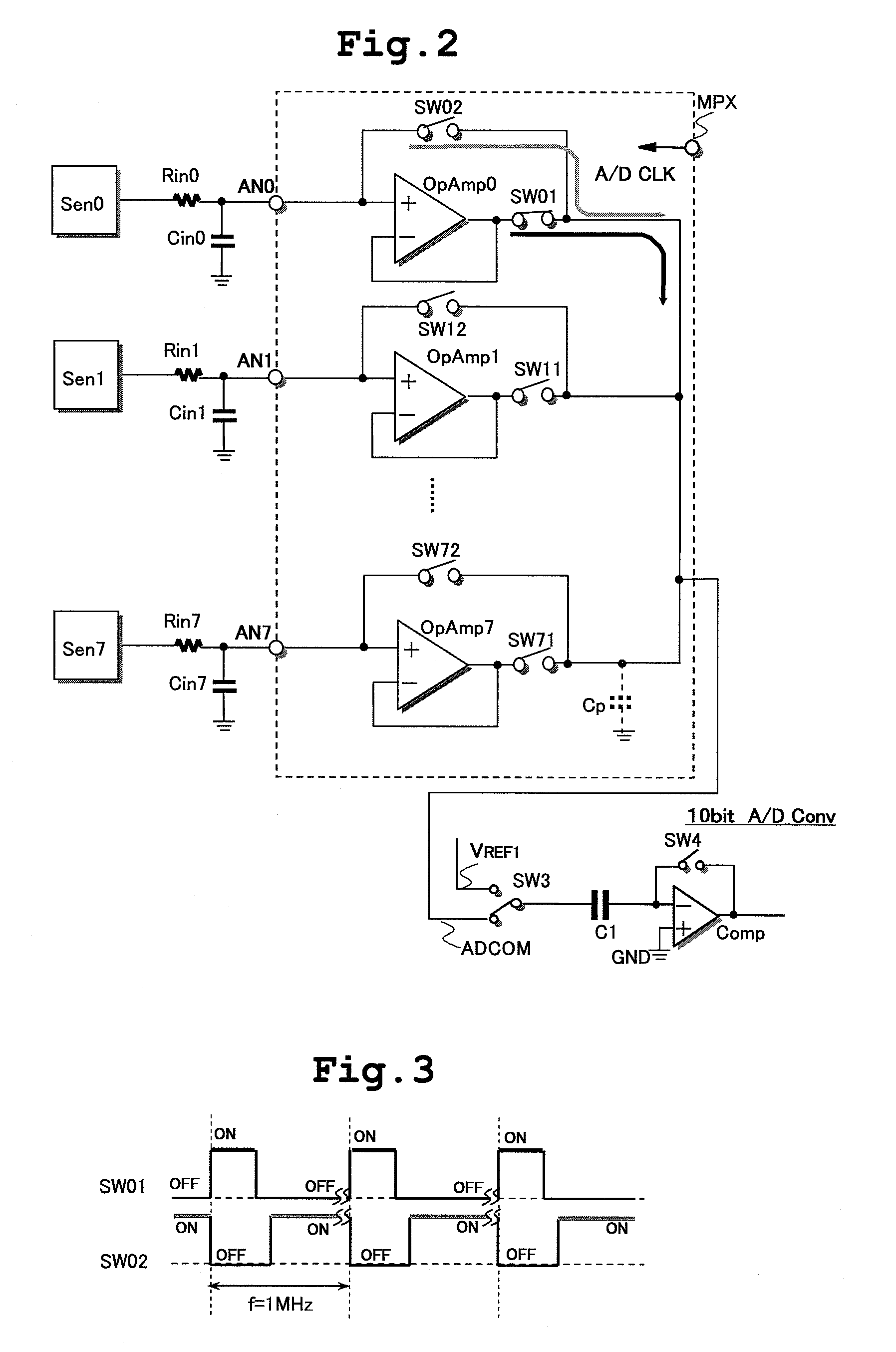
[0082]The sampling circuit includes an analog input terminal (AN0), an operational amplifier (OpAmp0), a first switch (SW01), a second switch (SW02), a third switch (SW03), a fourth switch (SW04), a fifth switch (SW05), and an analog output terminal (ADCOM).

[0083]The analog input terminal is coupled to one end of the first switch and one end of the second switch, and the other end of the first switch and the other end o...


PUM


Abstract

The present invention is directed to reduce offset error voltage in a signal source impedance of analog input signal voltage supplied to an input terminal due to input offset voltage of an operational amplifier in a sampling circuit or a multiplexer coupled to an input terminal of an A / D converter. A semiconductor integrated circuit has an A / D converter and a sampling circuit. The sampling circuit samples an analog input signal in first and second sample modes. The A / D converter converts the sampled analog signal to a digital signal in a conversion mode. By switching of an internal circuit of an operational amplifier between the first and second sample modes, the functions of a non-inverting input terminal (+) and an inverting input terminal (−) realized by first and second input terminals are switched. Synchronously with the switching, supply of an analog signal to the non-inverting input terminal by input switches is also switched.

Description

CLAIM OF PRIORITY[0001]The Present application claims priority from Japanese application JP 2007-309955 filed on Nov. 30, 2007, the content of which is hereby incorporated by reference into this application.FIELD OF THE INVENTION[0002]The present invention relates to a semiconductor integrated circuit and, more particularly, to a technique useful to reduce offset error voltage in analog input signal source impedance due to input offset voltage of an operational amplifier in a sampling circuit or a multiplexer coupled to an input terminal of an A / D converter.BACKGROUND OF THE INVENTION[0003]In a system requested to have high precision and high resolution, as described in the following non-patent document 1, an analog multiplexer is used for selecting one of a plurality of analog input signals and supplying it to an A / D converter for converting an analog signal to a digital signal. A plurality of analog input signals are supplied to one end of a plurality of analog switches in the ana...

Claims


Application Information

Patent Timeline
Patent Type & Authority Applications(United States)
IPC IPC(8): H03F1/08
CPCH03F3/45192H03F3/45475H03F3/45753H03F3/45977H03F2203/45138H03M3/342H03F2203/45726H03M1/0663H03M1/1225H03M1/46H03F2203/45212
Inventor KITAGAWA, AKIRAKITAGAWA, AKIHIRO
Owner RENESAS ELECTRONICS CORP
Why Eureka
Try Eureka