Power element mounting substrate, method of manufacturing the same, power element mounting unit, method of manufacturing the same, and power module

a technology of mounting substrate and power element, which is applied in the direction of conductive pattern formation, circuit layer/solid-state device details, lighting and heating apparatus, etc., can solve the problems of difference in flexural rigidity of circuit layer and cooler, easy cracking of solder layer between circuit layer and power element, and easy cracking of solder layer during heat cycle. , the effect of preventing the generation of warping during the formation of the power element mounting uni

Active Publication Date: 2009-06-11
MITSUBISHI MATERIALS CORP
View PDF12 Cites 13 Cited by
  • Summary
  • Abstract
  • Description
  • Claims
  • Application Information

AI Technical Summary

Benefits of technology

[0061]According to the power element mounting substrate of the invention, even if a lead-free solder material is used to solder the circuit layer and a power element, easy development of the crack in the solder layer during the heat cycle can be prevented.
[0062]According to the power element mounting unit of the invention in which the cooler having the cooling channel formed therein is brazed on the back surface, even if the cooler is brazed directly on the back surface of the ceramic plate, generation of warping during the formation of the power element mounting unit can be prevented. Thus, decrease in reliability on the heat cycle can be avoided.
[0063]According to the power element mounting unit in which the cooler includes the top plate section and the p

Problems solved by technology

A crack may easily develop in a solder layer between the circuit layer and the power element when the power module is subject to a heat cycle.
In the conventional power element mounting unit, difference in flexural rigidity of the circuit layer and the cooler is large and thus warping easily occurs d

Method used


Image

  • Power element mounting substrate, method of manufacturing the same, power element mounting unit, method of manufacturing the same, and power module
  • Power element mounting substrate, method of manufacturing the same, power element mounting unit, method of manufacturing the same, and power module
  • Power element mounting substrate, method of manufacturing the same, power element mounting unit, method of manufacturing the same, and power module

Examples


Embodiment Construction

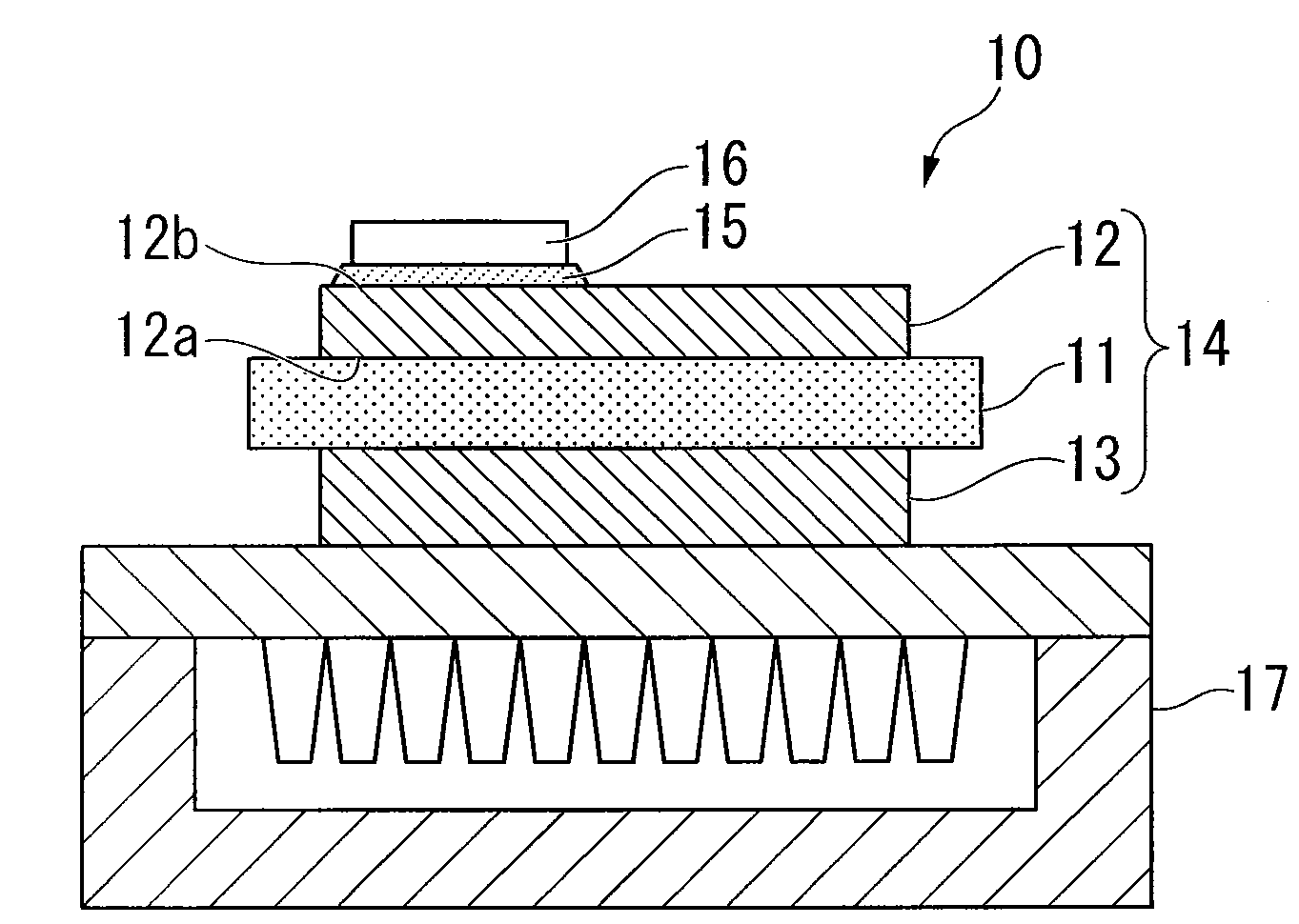
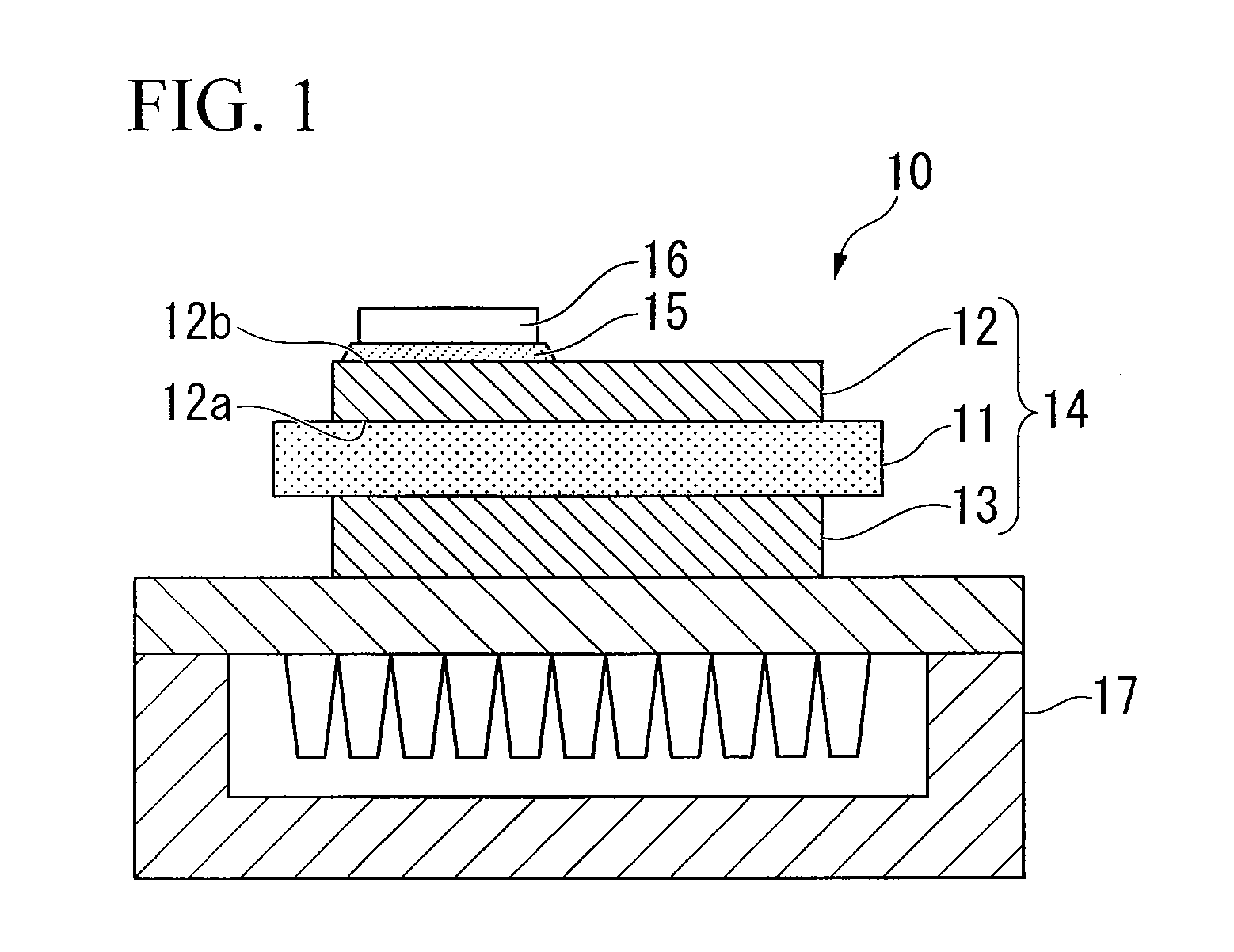
[0125]Referring now to the drawings, embodiments of the invention will be described. FIG. 1 is an overall view of a power module in which a power element mounting substrate according to an embodiment of the invention is used.

[0126]This power module 10 includes a power element mounting substrate 14, a semiconductor chip (power element) 16 and a heat sink 17. In the power element mounting substrate 14, a circuit layer 12 is brazed to a front surface of a ceramic plate 11 and a metal layer 13 is brazed to a back surface of the ceramic plate 11. The semiconductor chip (power element) 16 is soldered to a front surface of the circuit layer 12 via a solder layer 15. The heat sink 17 is brazed or soldered to a surface of the metal layer 13.

[0127]The ceramic plate 11 may be made of AlN, Al2O3, Si3N4 and SiC. The heat sink 17 may be made of pure Al, pure Cu, Al alloy, or Cu alloy. The solder layer 15 may be made of a lead-free solder material such as Sn—Ag—Cu-containing material. A brazing ma...


PUM

PropertyMeasurementUnit
Fractionaaaaaaaaaa
Fractionaaaaaaaaaa
Thicknessaaaaaaaaaa

Abstract

A power element mounting substrate including a circuit layer brazed to a surface of a ceramic plate, and a power element soldered to a front surface of the circuit layer, wherein the circuit layer is constituted using an Al alloy with an average purity of more than or equal to 98.0 wt % and less than or equal to 99.9 wt %, Fe concentration of the circuit layer at a side of a surface to be brazed to the ceramic plate is less than 0.1 wt %, and Fe concentration of the circuit layer at a side of the surface opposite to the surface to be brazed is more than or equal to 0.1 wt %.

Description

BACKGROUND OF THE INVENTION[0001]1. Field of the Invention[0002]The present invention relates to a power element mounting substrate, a method of manufacturing the same, a power element mounting unit, a method of manufacturing the same, and a power module, which are used in a semiconductor device for controlling high current and high voltage.[0003]This application claims priority of Japanese Patent Application No. 2006-157124 filed Jun. 6, 2006, Japanese Patent Application No. 2006-157125 filed Jun. 6, 2006, Japanese Patent Application No. 2006-169838 filed Jun. 20, 2006, Japanese Patent Application No. 2006-191468 filed Jul. 12, 2006, Japanese Patent Application No. 2006-224112 filed Aug. 21, 2006, and Japanese Patent Application No. 2007-61640 filed Mar. 12, 2007, the contents of which are incorporated herein by reference in their entirety.[0004]2. Background Art[0005]As shown in the below-listed Patent Document 1, such a power module generally includes a power element mounting sub...

Claims


Application Information

Patent Timeline
IPC IPC(8): H05K1/03H05K3/10
CPCH01L23/3735H01L23/3736H01L23/473H05K1/09Y10T29/49124H05K2201/0269H01L24/32H01L2224/32225H05K3/38H01L2224/2612
Inventor KUROMITSU, YOSHIROUISHIZUKA, HIROYAMIYATA, HIROSHIKITAHARA, TAKESHITONOMURA, HIROSHI
Owner MITSUBISHI MATERIALS CORP
Why Eureka
Try Eureka