Conductive pattern forming ink, conductive pattern, and wiring substrate
- Summary
- Abstract
- Description
- Claims
- Application Information
AI Technical Summary
Benefits of technology
Problems solved by technology
Method used
Image
Examples
first embodiment
[0050]Conductive Pattern Forming Ink
[0051]A conductive pattern forming ink according to a first embodiment of the invention is used for forming a conductive pattern on a substrate, especially used for forming a conductive pattern by a droplet discharge method.
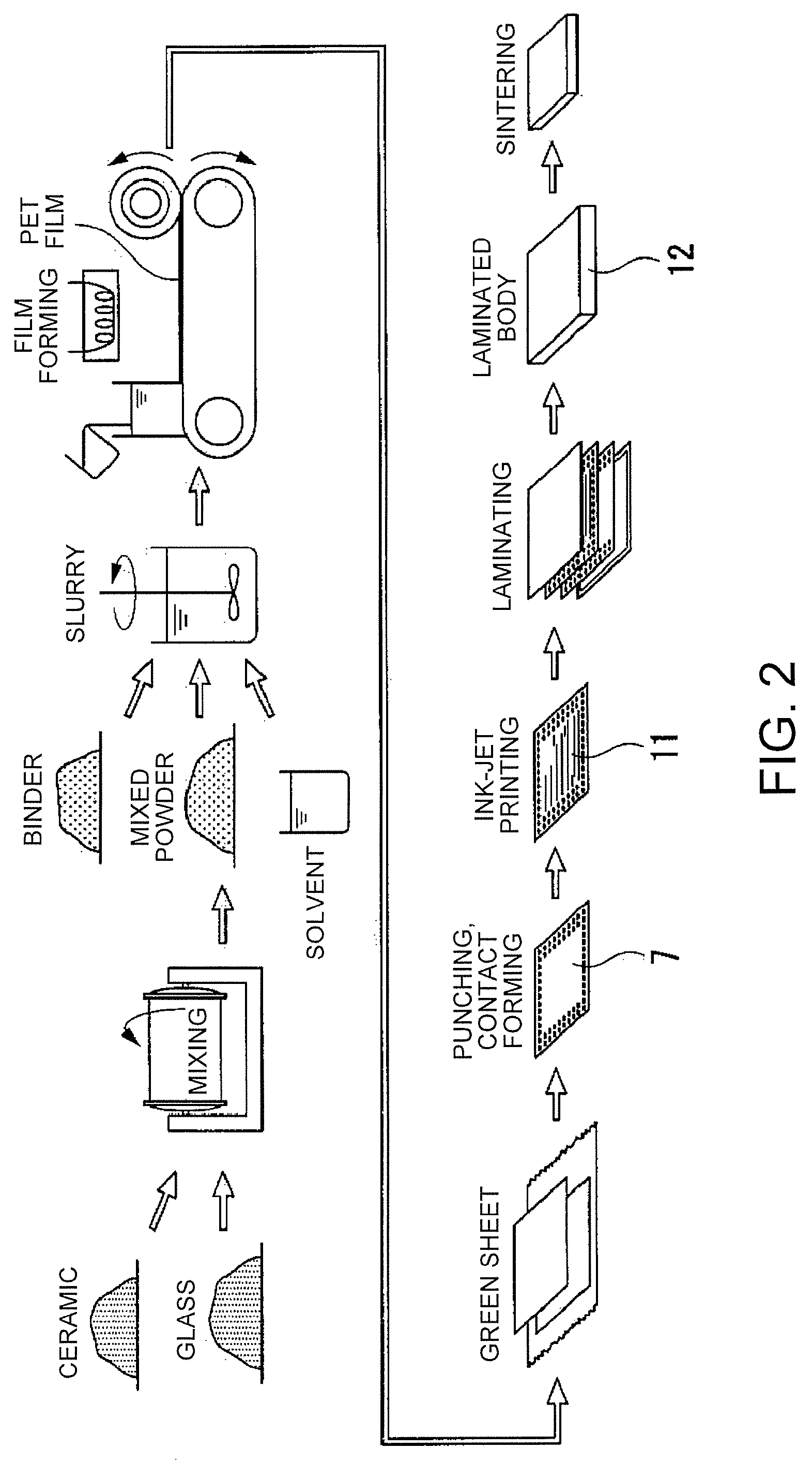
[0052]Any substrate may be used as a substrate on which a conductive pattern is formed. However, a ceramic substrate mainly made of ceramic is employed as the substrate in the embodiment. Further, the first embodiment will be explained by exemplifying a case where the conductive pattern forming ink is applied to a ceramic formed body (a ceramic green sheet) made of ceramic and a material containing a binder and having a sheet-like shape. Here, the ceramic formed body and the ink applied to the ceramic formed body undergo a sintering step as described later so as to be a ceramic substrate and a conductive pattern respectively.
[0053]The conductive pattern forming ink will now be described. In the embodiment, a case using a disper...
second embodiment
[0127]Method for Producing Conductive Pattern Forming Ink
[0128]An example of a method for producing a conductive pattern forming ink such as the ink described above will now be described as a second embodiment of the invention.
[0129]In the second embodiment, the conductive pattern forming ink is a colloidal liquid obtained by dispersing silver colloidal particles in an aqueous dispersion medium.
[0130]In producing a conductive pattern forming ink, an aqueous solution in which a dispersant and a reducing agent are dissolved is first prepared.
[0131]The dispersant is preferably blended in such amount that a molar ratio between silver of silver salt such as silver nitrate which is a starting substance and the dispersant is set to be about 1:1 to about 1:100. If the molar ratio of the dispersant with respect to silver salt is increased, a particle diameter of the silver particles is decreased. Therefore, contact points between the particles in the formed conductive pattern are increased, ...
third embodiment
[0155]Conductive Pattern
[0156]A conductive pattern according to a third embodiment of the invention will now be described.
[0157]The conductive pattern is formed by applying the ink described above on the ceramic formed body and then heating the ceramic formed body so as to have a thin film shape. On the conductive pattern, the silver particles are bonded to each other. The silver particles are bonded to each other with no space therebetween at least on the surface of the conductive pattern.
[0158]Especially, the conductive pattern is formed by using the conductive pattern forming ink of the first embodiment, so that disconnection caused by discharge defects, contact between the conductive patterns that are adjacent to each other, and the like are prevented. Accordingly, the conductive pattern is homogenized without cracks and disconnections so as to be highly reliable.
[0159]The conductive pattern of the third embodiment is formed such that the ink described above is applied on the ce...
PUM
| Property | Measurement | Unit |
|---|---|---|
| Acidity | aaaaa | aaaaa |
| Electrical conductor | aaaaa | aaaaa |
Abstract
Description
Claims
Application Information


