Photovoltaic device having a textured metal silicide layer

a technology of metal silicide layer and photovoltaic device, which is applied in the field of semiconductor devices, can solve the problems of significant price increases in the final solar cell module, the shortage of raw polysilicon feedstock used in the manufacture of silicon-based solar cells, and the inability to meet the requirements of photovoltaic energy generation, etc., and achieve the goal of developing less expensive photovoltaic modules

Inactive Publication Date: 2009-06-25
WOODSIDE GRP PTE LTD THE
View PDF12 Cites 26 Cited by
  • Summary
  • Abstract
  • Description
  • Claims
  • Application Information

AI Technical Summary

Problems solved by technology

In recent years, the high demand for silicon-based solar cells has created a shortage in the raw polysilicon feedstock used to manufacture these cells.
This shortage has resulted in significant price increases in the final solar cell modules.
Consequently, considerable effort has been expended in the art towards developing less expensive photovoltaic modules.
However, these approaches frequently yield lower efficiency solar cells, or suffer from volume manufacturing issues.
While the foregoing processes have been moderately successful in creating lab-scale solar cells, none has reached commercial production levels.
In the case of the ELTRAN® process, this failure is believed to arise, at least in part, from the presence of defects in the epitaxial layers.
However, front side texturing increases the dark current and, therefore, reduces the open circuit voltage (Voc) and the fill factor of a solar cell.
However, conventional backside texturing has its own challenges, since the front side has to be masked while the backside is etched for texturing.
This process is complicated by the fact that the alloying or sintering steps create a deep graded layer at the metal-semiconductor interface that actually absorbs photons rather than reflecting them back into the semiconductor where they can be used for generating electron-hole pairs.
However, in order to do this, one has to create gaps in the oxide film to dope the base region heavily and to diffuse the metal locally in order to form the rear contact.

Method used


Image

  • Photovoltaic device having a textured metal silicide layer
  • Photovoltaic device having a textured metal silicide layer
  • Photovoltaic device having a textured metal silicide layer

Examples


Embodiment Construction

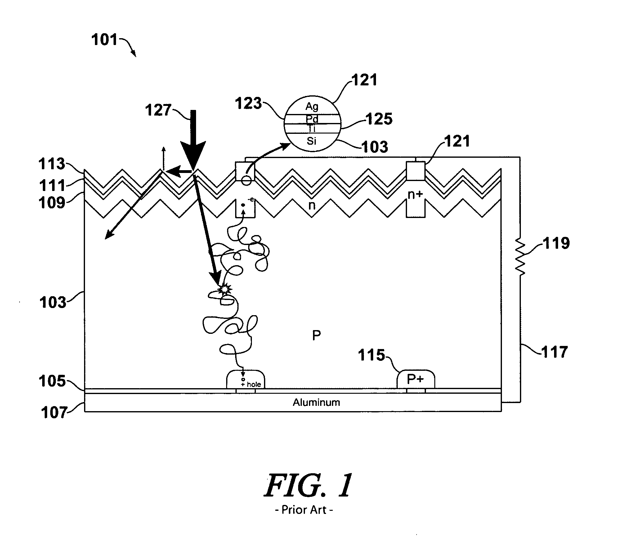
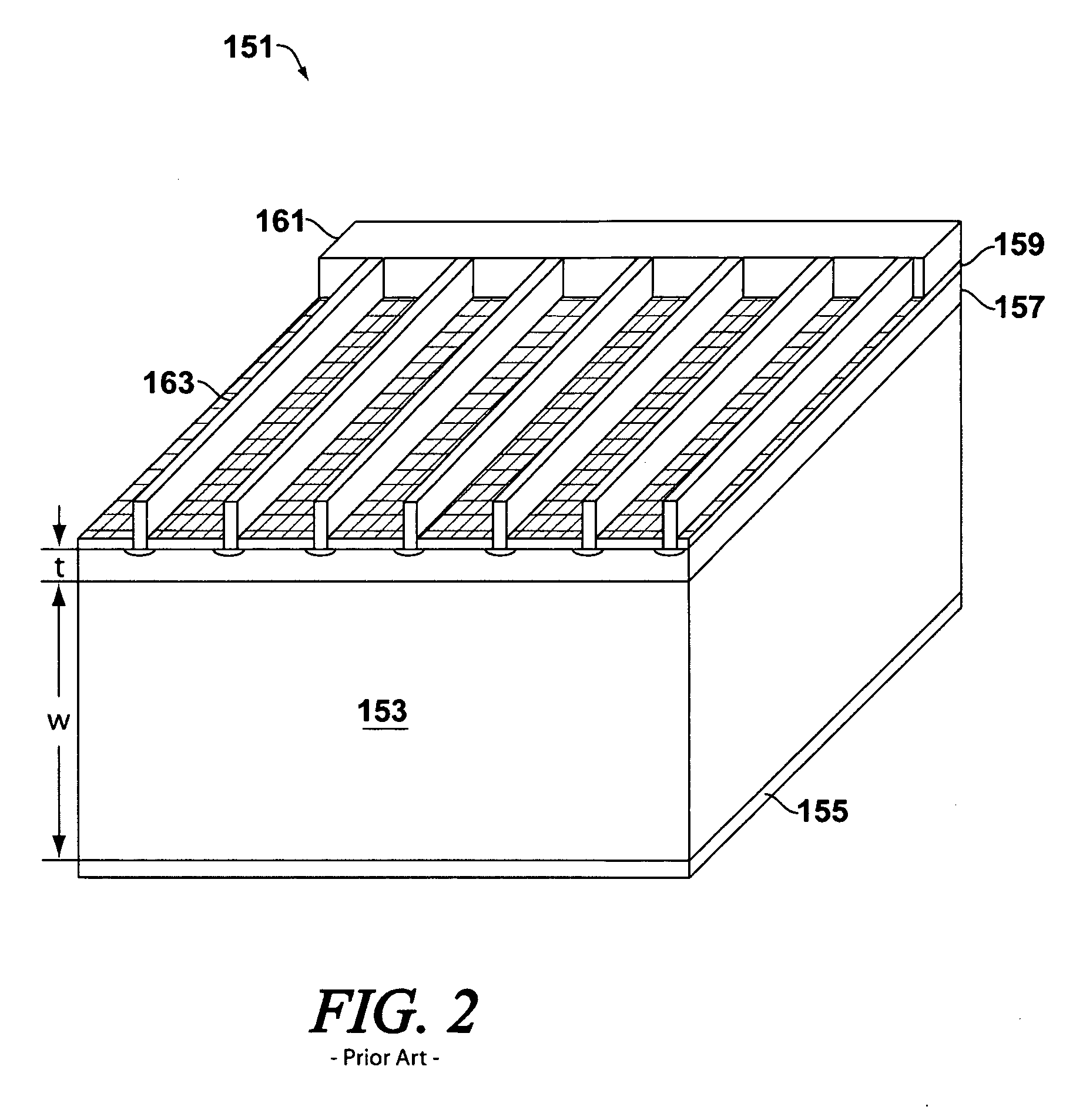
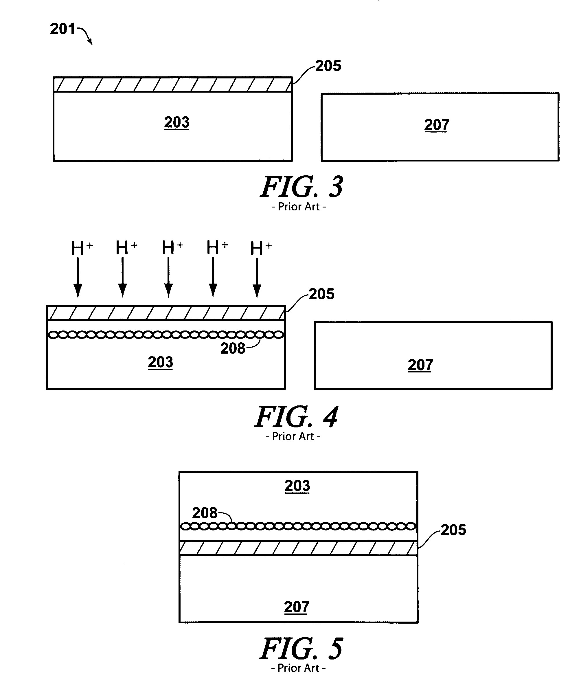
[0033]It has now been found that the aforementioned needs in the art may be met through the use of metal silicides or other metal-semiconductor intermetallic compounds to fabricate solar cells. Such materials may be utilized to simultaneously create a bonding agent, a back surface field (BSF), an optical reflecting layer, and / or a low resistivity rear ohmic contact in solar cell structures. The methodologies described herein may be utilized to fabricate low cost thin film solar cells having high efficiency, and may also be employed to create structures having multiple solar cells disposed on a common substrate, wherein the cells themselves may be fabricated using other techniques and structures as are known to the art.

[0034]By way of example, devices may be made in accordance with the teachings herein by a process which includes (a) splitting a semiconducting thin film from a semiconductor substrate; (b) depositing a metal film on a handle substrate such as stainless steel, metal fo...


PUM

PropertyMeasurementUnit
depthaaaaaaaaaa
depthaaaaaaaaaa
depthaaaaaaaaaa

Abstract

A semiconductor device is formed on a low cost substrate 312 onto which is deposited a metal film 314 that serves as an intermediate bonding layer with a transferred film 324 of semiconducting material from a bulk semiconductor substrate 322. The metal film forms an intermetallic compound such as a silicide 316 and functions as a bonding agent between the low cost substrate and the semiconducting substrate, as a back surface field for reflection of minority carriers, and as a textured optical reflector of photons. The silicide also forms a low resistivity back-side ohmic contact with the semiconductor layer. This results in a low cost, flexible, high efficiency, thin film solar cell device.

Description

FIELD OF THE DISCLOSURE[0001]The present disclosure relates generally to semiconductor devices, and more specifically to methods for fabricating solar cells.BACKGROUND OF THE DISCLOSURE[0002]Solar cells are devices that convert light energy into electrical energy by way of the photovoltaic effect. Solar cells operate through the photogeneration of charge carriers (electrons and holes) in absorbing material. The charge carriers so produced are then collected by conductive contacts to produce an electrical current.[0003]FIG. 1 depicts one known type of solar cell. A description of this cell may be found, for example, at http: / / en.wikipedia.org / wiki / Solar_cell). The solar cell 101 depicted therein is silicon based, and comprises a wafer 103 of p-type silicon. The wafer 103 is capped on one end with a layer of oxide 105, a region of p+ type silicon 115 and an aluminum back contact 107, and is capped on the other end with a layer of n-type silicon 109, a layer of SiO2 111 and an anti ref...

Claims


Application Information

Patent Timeline
Patent Type & Authority Applications(United States)
IPC IPC(8): H01L31/028H01L31/04
CPCH01L31/1804H01L31/1892H01L31/1896H01L31/056Y02E10/547H01L31/046Y02E10/52H01L31/042H01L31/0504Y02P70/50
Inventor JAWARANI, DHARMESHAGARWAL, VINOD KUMAR
Owner WOODSIDE GRP PTE LTD THE
Why Eureka
Try Eureka