Diode and display device including diode

a technology of diodes and diodes, applied in the direction of diodes, semiconductor devices, electrical equipment, etc., can solve the problems of increasing cost, reducing yield, and reducing the operation cost of polycrystalline semiconductor films, and achieves reduced off current of thin film transistors, high field effect mobility, and large amount of on current

Inactive Publication Date: 2009-06-25
SEMICON ENERGY LAB CO LTD
View PDF26 Cites 44 Cited by
  • Summary
  • Abstract
  • Description
  • Claims
  • Application Information

AI Technical Summary

Benefits of technology

[0008]In addition, an inverted staggered thin film transistor using a microcrystalline semiconductor film for a channel formation region can have a larger amount of on current than an inverted staggered thin film transistor using an amorphous semiconductor film for a channel formation region; however, the inverted staggered thin film transistor using a microcrystalline semiconductor film for a channel formation region has a larger amount of off current, too. A display device which uses a thin film transistor having a large amount of off current has problems that contrast is decreased and power consumption is increased.
[0009]In view of the above problems, it is an object of the present invention to reduce off current of a thin film transistor. It is another object of the present invention to reduce reverse bias current of a diode. It is another object of the present invention to improve image quality of a display device.
[0018]Further, a display device in which thin film transistors (TFTs) using a microcrystalline semiconductor film for a channel formation region is used for a pixel portion and a driver circuit is manufactured. Since a microcrystalline semiconductor film of the present invention has high crystallinity at the interface with a gate insulating film, the thin film transistor using the microcrystalline semiconductor film has a field effect mobility of from 2.5 cm2 / V·sec to 10 cm2 / V·sec, which is 5 to 20 times higher than that of the thin film transistor using an amorphous semiconductor film. Therefore, part of the driver circuit or the entire driver circuit can be formed over the same substrate as that of the pixel portion, so that a system-on-panel can be manufactured.
[0022]According to the present invention, off current of a thin film transistor can be reduced. Further, a thin film transistor with a large amount of on current, high field effect mobility, and a small amount of off current can be manufactured. Further, reverse bias current of a diode can be reduced. Furthermore, a diode which has high switching speed at the time of high voltage application can be manufactured. Therefore, image quality of a display device can be improved.

Problems solved by technology

However, the thin film transistor using a polycrystalline semiconductor film requires a more complicated process than the thin film transistor using an amorphous semiconductor film because of crystallization of the semiconductor film.
Thus, there are problems such as a reduction in yield and an increase in cost.
A display device which uses a thin film transistor having a large amount of off current has problems that contrast is decreased and power consumption is increased.

Method used


Image

  • Diode and display device including diode
  • Diode and display device including diode
  • Diode and display device including diode

Examples


embodiment mode 1

[0058]In this embodiment mode, a manufacturing process of a thin film transistor with high mobility, a large amount of on current, and a small amount of off current is described below. In this embodiment mode, manufacturing processes of a thin film transistor, a pixel electrode, and a capacitor element which are formed in each pixel of a pixel portion 1331 in the top view of an element substrate 1300 of a display device illustrated in FIG. 14 are described below.

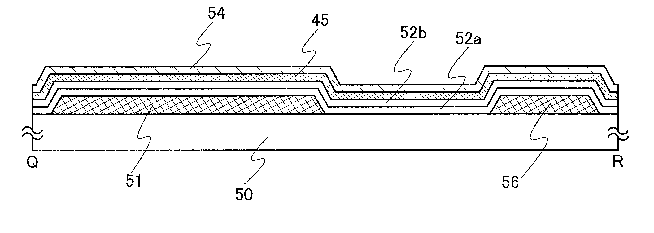
[0059]Enlarged views of a region connected to a thin film transistor and a pixel electrode of one pixel of the pixel portion 1331 in FIG. 14 are illustrated in FIGS. 5A to 5D, cross-sectional views taken along a line Q-R in FIGS. 5A to 5D are illustrated in FIGS. 1A to 1C, FIGS. 2A to 2C, and FIGS. 3A to 3C, and cross-sectional views taken along a line S-T in FIGS. 5A to 5D are illustrated in FIGS. 4A to 4C.

[0060]As illustrated in FIG. 1A, a gate electrode 51 and a capacitor wiring 56 are formed over a substrate 50, and gate...

embodiment mode 2

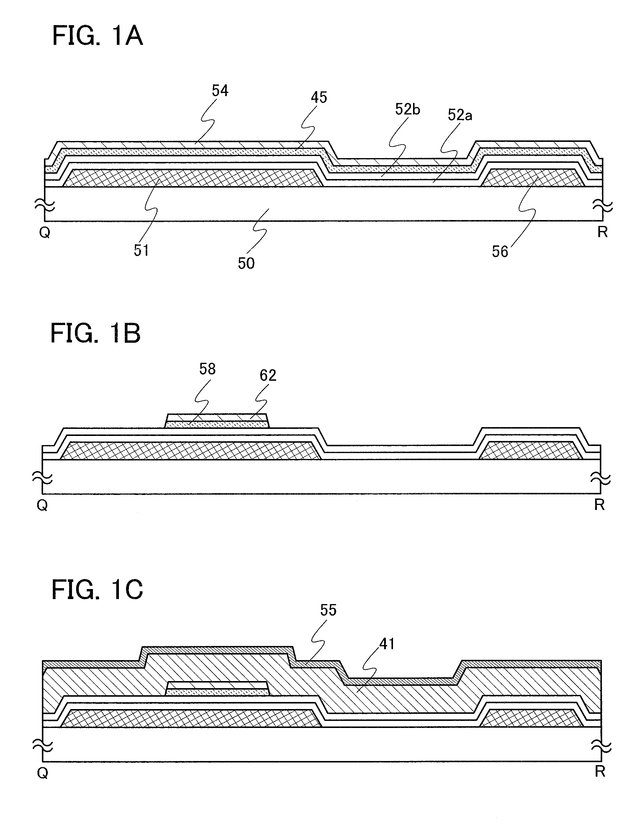
[0120]In this embodiment mode, a process for manufacturing a thin film transistor using a process capable of reducing the number of photomasks compared with Embodiment Mode 1 is described.

[0121]In a similar manner to Embodiment Mode 1, as illustrated in FIG. 6A, a conductive film is formed over the substrate 50, a resist is applied over the conductive film, and the conductive film is partly etched using a resist mask formed through a photolithography process using the first photomask, so that the gate electrode 51 and the capacitor wiring 56 are formed. Subsequently, the gate insulating films 52a and 52b are formed over the gate electrode 51. Then, the microcrystalline semiconductor film 58 which includes the impurity element serving as a donor and the first buffer layer 62 are formed over the gate insulating film 52 through a photolithography process using the second photomask. Next, the second buffer layer 41, the impurity semiconductor film 55 to which the impurity element impart...

embodiment mode 3

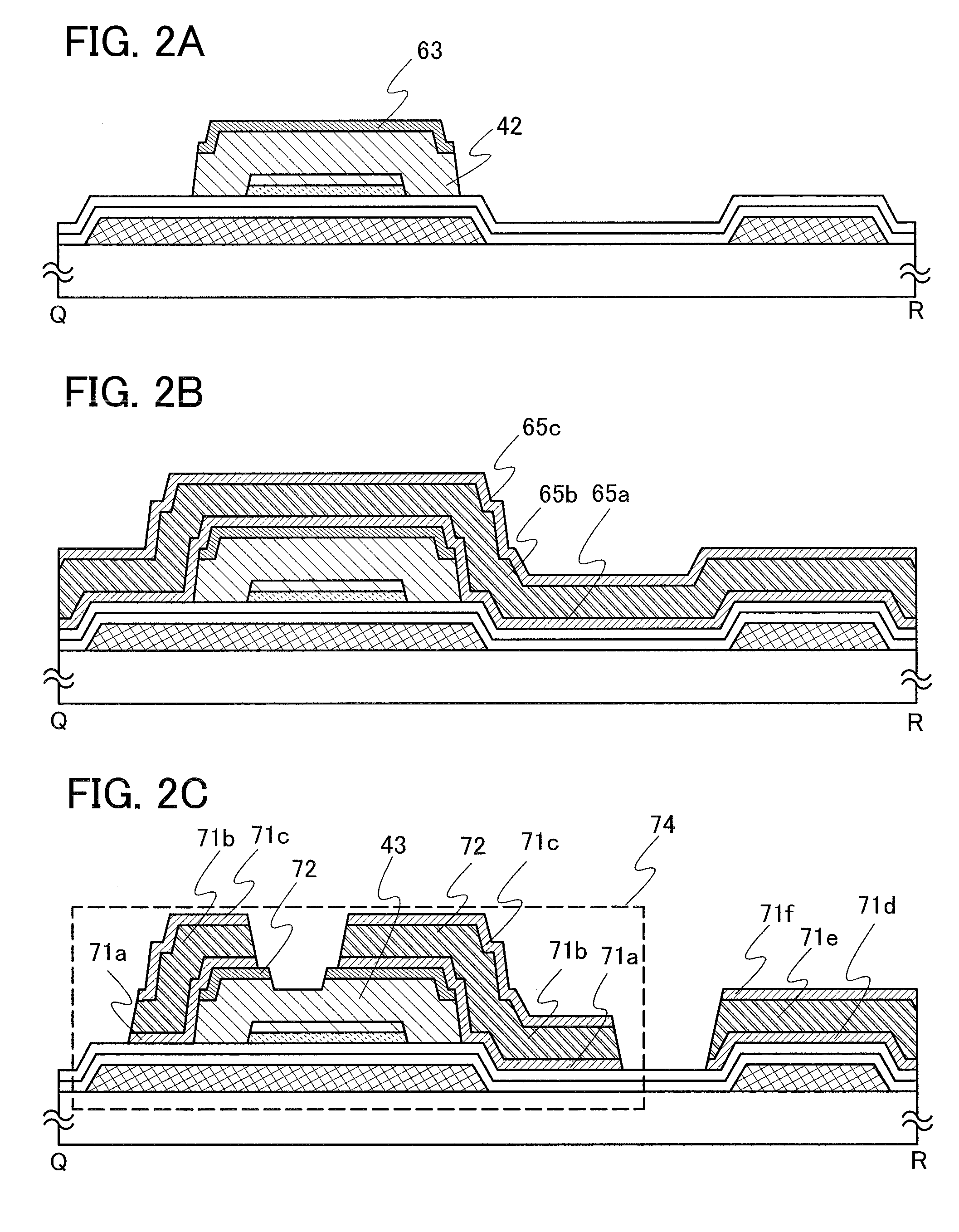
[0145]In this embodiment mode, a mode which is different from the thin film transistors in Embodiment Modes 1 and 2 is described.

[0146]FIG. 10 illustrates a mode of thin film transistor in which crystal grains 60 which include an impurity element serving as a donor are dispersed over the gate insulating film 52b, and the crystal grains 60 which include the impurity element serving as a donor and a semiconductor film 61 which covers the crystal grains 60 which include the impurity element serving as a donor and the gate insulating film 52b and contains germanium as its main component are included instead of the microcrystalline semiconductor film which includes the impurity element serving as a donor of the thin film transistors shown in Embodiment Modes 1 and 2. In addition, the second buffer layer 43 which covers top and side surfaces of the semiconductor film 61 which contains germanium as its main component is formed. Compared with the crystal grains 60 which contains silicon as ...


PUM


Abstract

A thin film transistor which includes a microcrystalline semiconductor film over a gate electrode with a gate insulating film interposed therebetween to be in an inner region in which end portions of microcrystalline semiconductor film are in an inside of end portions of the gate electrode, an amorphous semiconductor film which covers top and side surfaces of the microcrystalline semiconductor film, and an impurity semiconductor film to which an impurity element imparting one conductivity is added, and which forms a source region and a drain region, wherein the microcrystalline semiconductor film includes an impurity element serving as a donor is provided to reduce off current of a thin film transistor, to reduce reverse bias current of a diode, and to improve an image quality of a display device using a thin film transistor.

Description

BACKGROUND OF THE INVENTION[0001]1. Field of the Invention[0002]The present invention relates to a diode and a display device including the diode.[0003]2. Description of the Related Art[0004]In recent years, techniques to form thin film transistors using a semiconductor thin film (with a thickness of approximately several tens to several hundreds of nanometers) which is formed over a substrate having an insulating surface have attracted attention. A thin film transistor is broadly applied to electronic devices such as an IC and an electrooptic device, and particularly, a thin film transistor as a switching element of an image display device is expected to be developed quickly.[0005]A thin film transistor using an amorphous semiconductor film, a thin film transistor using a polycrystalline semiconductor film in which a diameter of the crystal grain is 100 nm or more, or the like is used as a switching element in an image display device. As a method of forming a polycrystalline semico...

Claims


Application Information

Patent Timeline
Patent Type & Authority Applications(United States)
IPC IPC(8): H01L29/861H01L29/04
CPCH01L29/04H01L29/458H01L29/4908H01L27/124H01L29/78696H01L27/1222H01L29/66765H01L29/86
Inventor YAMAZAKI, SHUNPEIHOSOYA, KUNIOSUZUKI, YASUTAKAFUJIKAWA, SAISHI
Owner SEMICON ENERGY LAB CO LTD
Why Eureka
Try Eureka