Organic light emitting device

Active Publication Date: 2009-06-25
SAMSUNG DISPLAY CO LTD
View PDF28 Cites 20 Cited by
  • Summary
  • Abstract
  • Description
  • Claims
  • Application Information

AI Technical Summary

Benefits of technology

[0007]Aspects of the present invention provide an organic light emitting device having reduced power consumption, improved driving vol

Problems solved by technology

In addition, conventional organic light emitting devices are limited in terms of the amoun

Method used


Image

  • Organic light emitting device
  • Organic light emitting device
  • Organic light emitting device

Examples


example 1

Manufacture of Organic Light Emitting Device

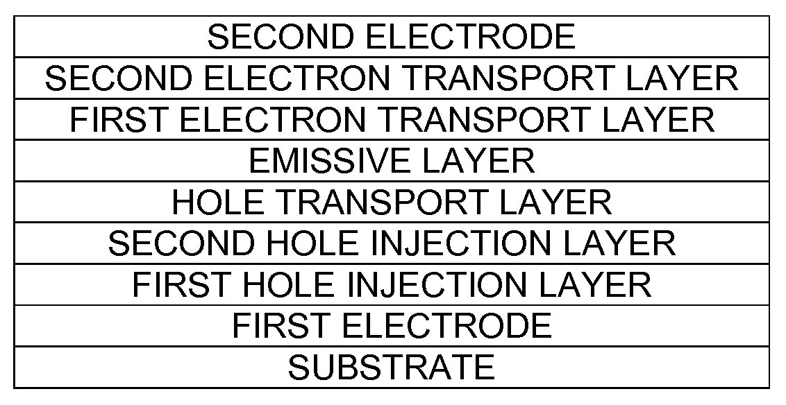
[0074]As an anode, a Corning 15 Ω / cm2 (1200 Å) ITO glass substrate was cut to a size of 50 mm×50 mm×0.7 mm and was ultrasonically washed with isopropyl alcohol and pure water for 5 minutes, respectively. The ITO glass substrate was irradiated with ultraviolet rays for 30 minutes and washed with ozone.

[0075]Then, NPB and MoOX were co-deposited on the substrate to form a first hole injection layer with a thickness of 100 Å. Subsequently, TCTA was coated on the first hole injection layer to form a second hole injection layer.

[0076]NPB was vacuum deposited on the second hole injection layer to form a hole transport layer having a thickness of 60 nm. After the formation of the hole transport layer, 100 parts by weight of Alq3 as a host and 5 parts by weight of coumarin 6 as a dopant were vacuum deposited on the hole transport layer to form an emissive layer.

[0077]Then, 30 parts by weight of LiF and 70 parts by weight of BeBq2 were vacuum co-dep...

example 2

Manufacture of Organic Light Emitting Device

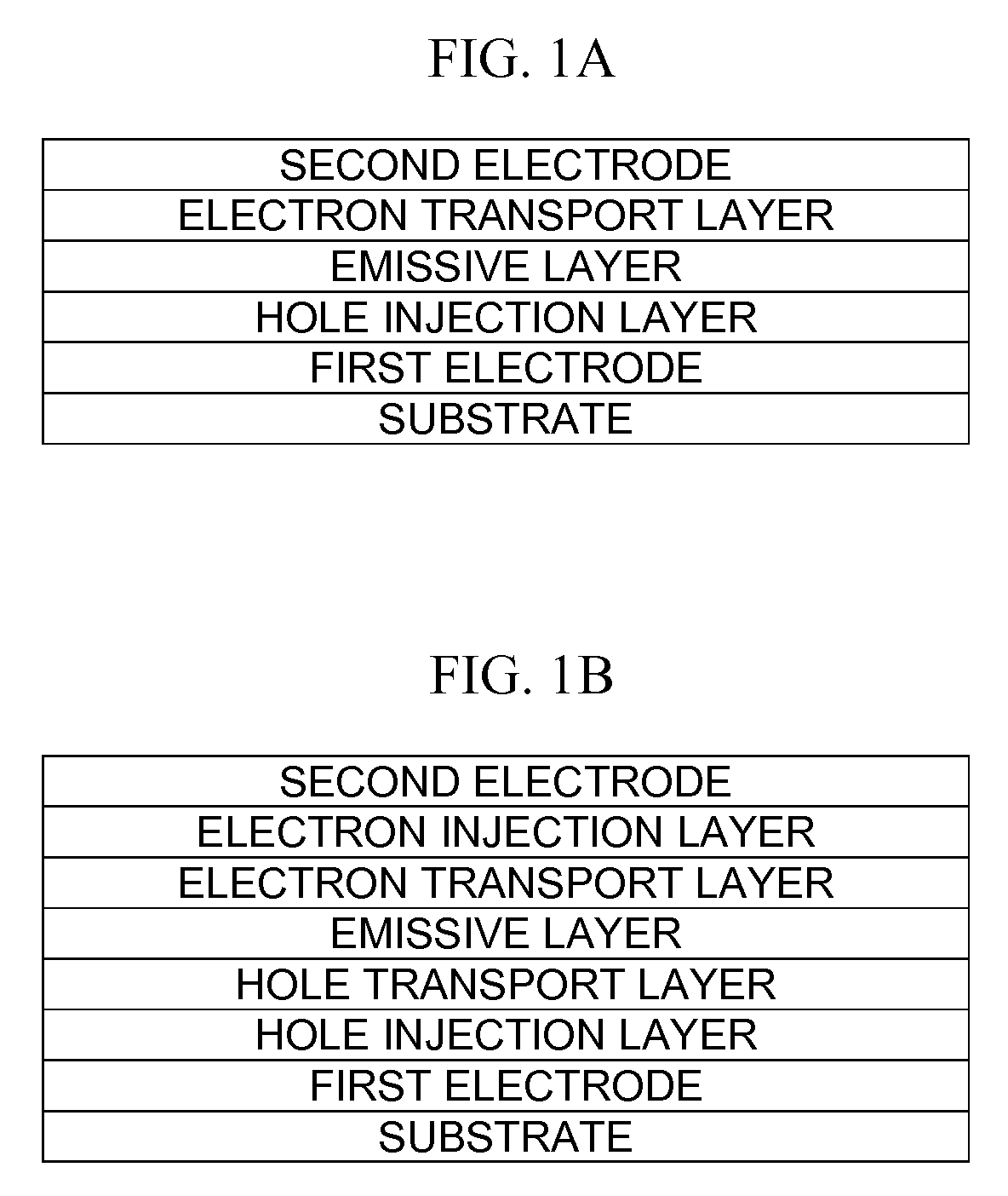
[0079]An organic light emitting device was manufactured in the same manner as in Example 1, except that 50 parts by weight of lithium quinolate and 50 parts by weight of BeBq2 were vacuum co-deposited to form the electron transport layer.

example 3

Manufacture of Organic Light Emitting Device

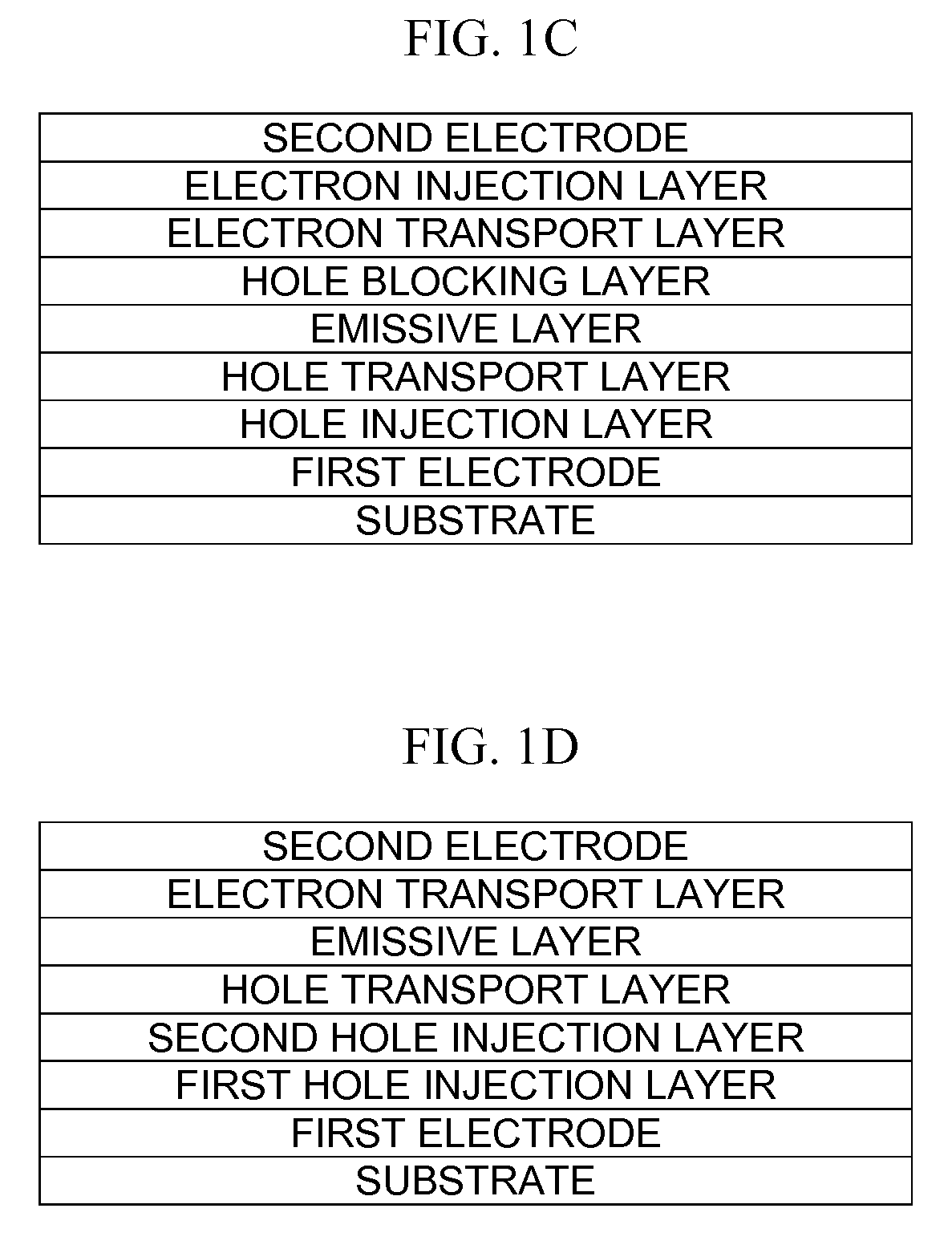
[0080]As an anode, a Corning 15 Ω / cm2 (1200 Å) ITO glass substrate was cut to a size of 50 mm×50 mm×0.7 mm and was ultrasonically washed with isopropyl alcohol and pure water for 5 minutes, respectively. The ITO glass substrate was irradiated with ultraviolet rays for 30 minutes and washed with ozone.

[0081]A hole injection layer formed of CuPc was formed on the substrate to a thickness of 5 nm.

[0082]NPB was vacuum deposited on the hole injection layer to form a hole transport layer having a thickness of 60 nm. After the formation of the hole transport layer, 100 parts by weight of Alq3 as a host and 5 parts by weight of coumarin 6 as a dopant were vacuum deposited on the hole transport layer to form an emissive layer.

[0083]Then, BeBq2 was vacuum deposited on the emissive layer to form a first electron transport layer (ETL1) having a thickness of 10 nm.

[0084]50 parts by weight of LiF and 50 parts by weight of BeBq2 were vacuum co-deposited ...


PUM

PropertyMeasurementUnit
Lengthaaaaaaaaaa
Percent by massaaaaaaaaaa

Abstract

An organic light emitting device includes a first electrode; a second electrode; an emissive layer disposed between the first electrode and the second electrode; a hole injection layer disposed between the first electrode and the emissive layer; and an electron transport layer disposed between the emissive layer and the second electrode. The hole injection layer includes a hole injecting material and a first compound made up of an element selected from the group consisting of Mo, Li, Na, K, Rb, Cs, Be, Mg, Ca, Sr, Ba, and B and an element selected from the group consisting of O, F, S, Cl, Se, Br, and I. The electron transport layer includes an electron transporting material and a second compound, wherein the second compound is represented by Formula 1:
XaYb   <Formula 1>
    • X is an alkali metal, an alkali earth metal, or a transition metal,
    • Y is a group 7 element, or a C1-C20 organic group,
    • a is a number in the range of 1 to 3, and
    • b is a number in the range of 1 to 3.

Description

CROSS-REFERENCE TO RELATED APPLICATIONS[0001]This application claims the benefit of Korean Patent Application No. 2007-136406, filed Dec. 24, 2007, in the Korean Intellectual Property Office, the disclosure of which is incorporated herein by reference.BACKGROUND OF THE INVENTION[0002]1. Field of the Invention[0003]Aspects of the present invention relate to an organic light emitting device, and more particularly, to an organic light emitting device with improved driving voltage, light emitting efficiency, lifetime, and the like by using a novel hole injecting material and a novel electron transporting material. In addition, aspects of the present invention may contribute to development of a high image quality organic light emitting device, and provides an organic light emitting device with reduced power consumption and improved lifetime.[0004]2. Description of the Related Art[0005]Organic light emitting devices are devices in which, when a current is supplied to an organic layer inte...

Claims


Application Information

Patent Timeline
IPC IPC(8): H05B33/00
CPCH01L51/5048H01L51/5092H01L51/5088H01L51/5052Y10T428/31504H10K50/14H10K50/155H10K50/165H10K50/171H10K50/17H05B33/20C09K11/06H10K50/00
Inventor SONG, WON-JUNSUNG, YEUN-JOOKIM, MU-HYUN
Owner SAMSUNG DISPLAY CO LTD
Why Eureka
Try Eureka