Multilayer ceramic electronic component and manufacturing method thereof

a technology of multi-layer ceramics and electronic components, which is applied in the direction of fixed capacitors, fixed capacitor details, coatings, etc., can solve the problems of difficult to ensure quality, restricted expansion of the effective area of the internal electrode, and restricted expansion of the ceramic layer within a predetermined dimensional standard, so as to improve the performance reduce the size of multi-layer ceramic electronic components, and increase the volume of the ceramic base body

Active Publication Date: 2009-06-25
MURATA MFG CO LTD
View PDF31 Cites 19 Cited by
  • Summary
  • Abstract
  • Description
  • Claims
  • Application Information

AI Technical Summary

Benefits of technology

[0026]In addition, since each of the Cu plating films included in the external terminal electrodes is formed by plating, compared to the case of using a conductive paste, the Cu plating film can be formed to be thin and flat. Hence, since the size of a multilayer ceramic electronic component can be reduced, and the volume of the ceramic base body can be increased within a predetermined dimensional standard, the performance of the multilayer ceramic electronic component can be improved. In particular, when the above Cu plating film is applied to a multilayer ceramic capacitor, the capacity can be increased within a predetermined dimensional standard.
[0027]In the case in which the above Cu oxides include Cu2O and CuO, the Cu oxides include Cu2O, which enables strong diffusion bonding with ceramic, preferably at approximately 90 percent by weight or more. Thereby, the bonding force of the external terminal electrodes to the ceramic base body can be further increased.
[0028]When the internal conductors include a dummy internal conductor, the bonding force of the external terminal electrodes to the ceramic base body can be further increased.
[0029]When auxiliary conductors are formed on external surfaces of the ceramic base body in regions in which the exposed portions of the internal electrodes are not formed, the external terminal electrodes can be easily extended, and as a result, the bonding force of the external terminal electrodes to the ceramic base body can be further increased.
[0030]When the ceramic base body has a first and a second side surface facing each other and a third and a fourth si

Problems solved by technology

A further decrease in the thickness of ceramic layers has been attempted but as the thickness of the ceramic layers is decreased, short-circuiting is liable to occur between internal electrodes, and as a result, it becomes disadvantageously difficult to ensure the quality.
Hence, an increase in effective area of the internal electrode is restricted.
However, an increase in the area of the ceramic layer within a predetermined dimensional st

Method used


Image

  • Multilayer ceramic electronic component and manufacturing method thereof
  • Multilayer ceramic electronic component and manufacturing method thereof
  • Multilayer ceramic electronic component and manufacturing method thereof

Examples


first embodiment

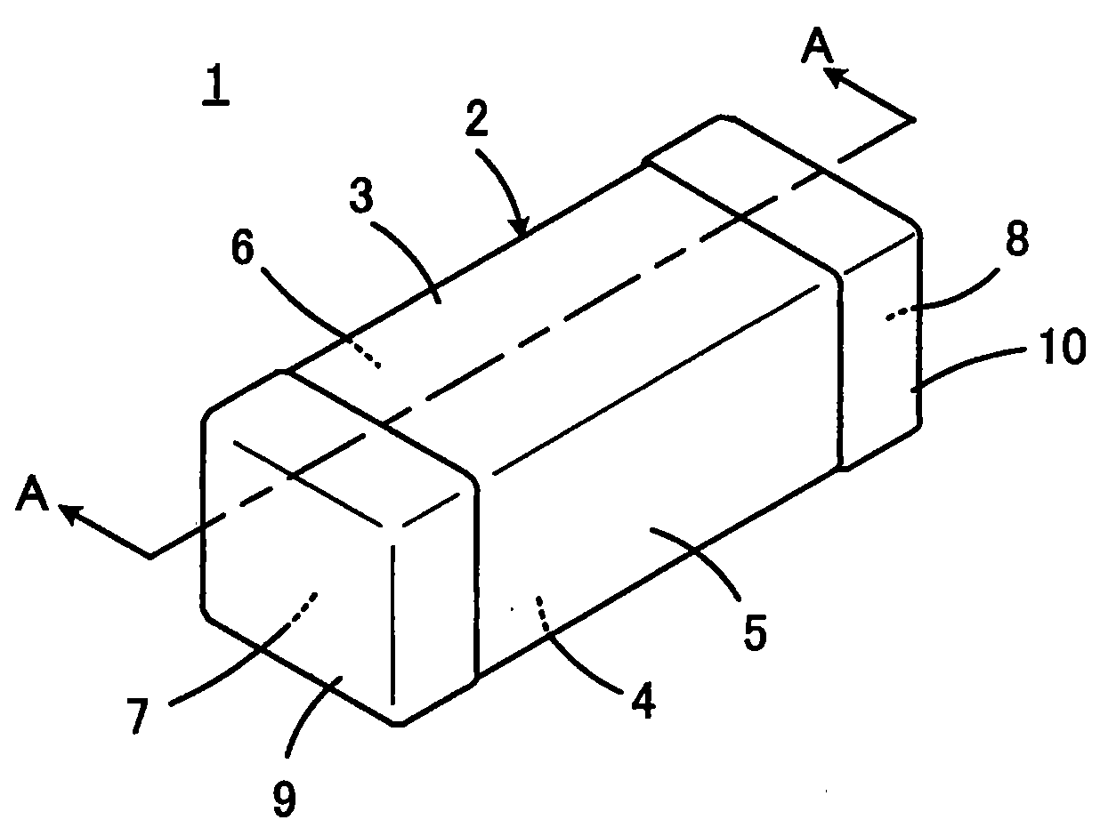
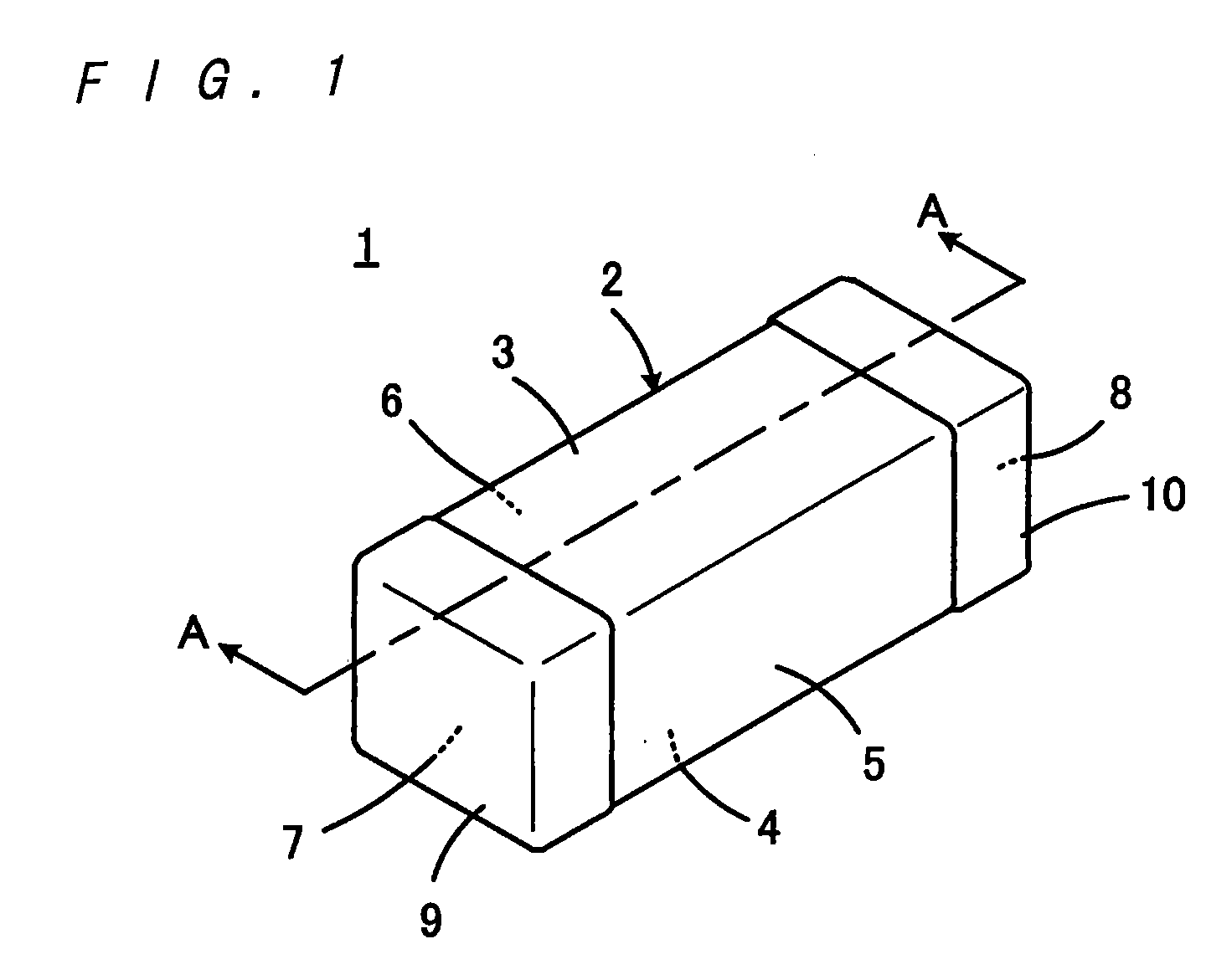
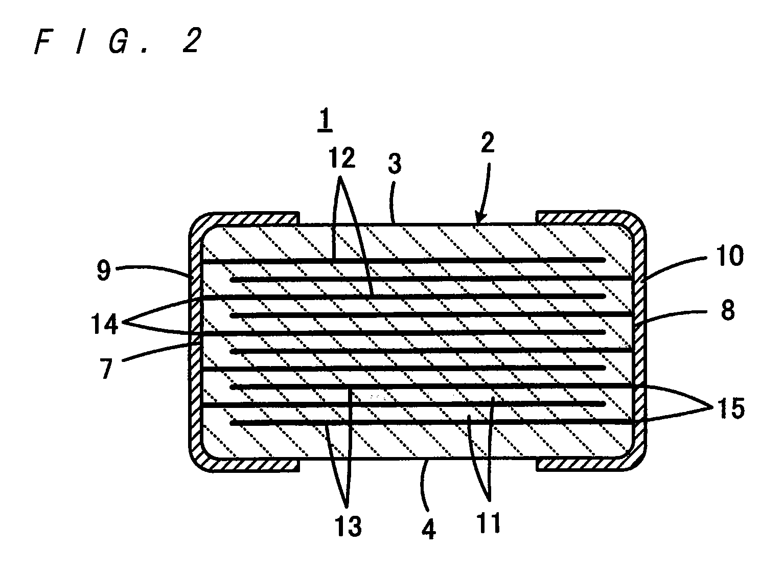
[0060]FIGS. 1 to 4 are views illustrating the present invention. FIG. 1 is a perspective view showing a multilayer ceramic capacitor 1 as one example of a multilayer ceramic electronic component. FIG. 2 is a cross-sectional view taken along the line A-A of FIG. 1.

[0061]The multilayer ceramic capacitor 1 has a ceramic base body 2. The ceramic base body 2 is in the shape of a substantially rectangular parallelepiped having a first and a second primary surface 3 and 4 facing each other, and four side surfaces 5 to 8 connecting the first and the second primary surfaces 3 and 4. In the following description, among the four side surfaces 5 to 8, the side surfaces 5 and 6 extending along the longer sides of the primary surfaces 3 and 4 are called a first and a second side surface, respectively, and the side surfaces 7 and 8 extending along the shorter sides of the primary surfaces 3 and 4 are called a first and a second end surface, respectively.

[0062]A first and a second external terminal...

second embodiment

[0083]FIG. 5 is a view corresponding to FIG. 4 and illustrating the present invention. In FIG. 5, elements corresponding to the elements shown in FIG. 4 are designated by the same reference numerals, and a duplicated description will be omitted.

[0084]In the second embodiment, a first outside conductive layer 24 and a second outside conductive layer 25 are further formed on each of the Cu plating films 20.

[0085]The first outside conductive layer 24 is composed of a metal selected from the group consisting of Cu and Ni or an alloy containing the metal of the group. The first outside conductive layer 24 functions as a barrier layer to prevent each of the Cu plating films 20 from being corroded by solder, which is used, for example, for mounting of the ceramic capacitor 1. In addition, when the first outside conductive layer 24 is composed of Cu, the Cu first outside conductive layer 24 increases the thickness of the Cu film of the Cu plating film 20 and functions as a barrier layer aga...

third embodiment

[0087]FIG. 6 is a view corresponding to FIG. 4 and illustrating the present invention. In FIG. 6, elements corresponding to the elements shown in FIG. 4 are designated by the same reference numerals, and a duplicated description will be omitted.

[0088]In the third embodiment, an outside conductive layer 28 is further formed on each of the Cu plating films 20. The outside conductive layer 28 is composed of one metal selected from the group consisting of Au, Ag, and Pd or an alloy containing a metal of the group. The third embodiment is advantageously used when the multilayer ceramic capacitor 1 is to be mounted not by soldering but by, for example, conductive adhesive or wire bonding. According to the third embodiment, compared to the second embodiment, the number of layers of each of the external terminal electrodes 9 and 10 can be decreased.


PUM

PropertyMeasurementUnit
Temperatureaaaaaaaaaa
Fractionaaaaaaaaaa
Timeaaaaaaaaaa

Abstract

A multilayer ceramic electronic component including thin external terminal electrodes each having a superior bonding force to a ceramic base body is provided. In order to form the external terminal electrodes, after Cu plating films are deposited on exposed portions of internal electrodes by direct plating on a ceramic base body, a Cu liquid phase, an O2-containing liquid phase, and a Cu solid phase are generated between the Cu plating film and the ceramic base body by a heat treatment, so that Cu oxides are dispersed in the Cu plating film, at least near an interface with the ceramic base body. Since the Cu oxides function as an adhesive, a bonding force of the Cu plating film to the ceramic base body can be increased, and hence the external terminal electrode having a superior bonding force to the ceramic base body can be obtained.

Description

BACKGROUND OF THE INVENTION[0001]1. Field of the Invention[0002]The present invention relates to a multilayer ceramic electronic component and a manufacturing method thereof, and more particularly relates to the structure of external terminal electrodes provided in a multilayer ceramic electronic component and a method for forming the external terminal electrodes.[0003]2. Description of Related Art[0004]In recent years, the market for compact portable electronic devices, such as mobile phones, notebook personal computers, digital cameras, and digital audio devices, has been expanded. In the field of portable electronic devices, reduction in size and improvement in performance have been simultaneously advanced. Many multilayer ceramic electronic components are mounted in one portable electronic device, and therefore, the multilayer ceramic electronic components are also required to be reduced in size and to be improved in performance. For example, a multilayer ceramic capacitor is re...

Claims


Application Information

Patent Timeline
IPC IPC(8): H01G4/12B05D5/12
CPCH01G4/005H01G4/232H01G4/12
Inventor TAKEUCHI, SHUNSUKEKAWASAKI, KENICHIMOTOKI, AKIHIROOGAWA, MAKOTOMATSUMOTO, SHUJINISHIHARA, SEIICHI
Owner MURATA MFG CO LTD
Why Eureka
Try Eureka