Apparatus and method for processing a substrate using inductively coupled plasma technology

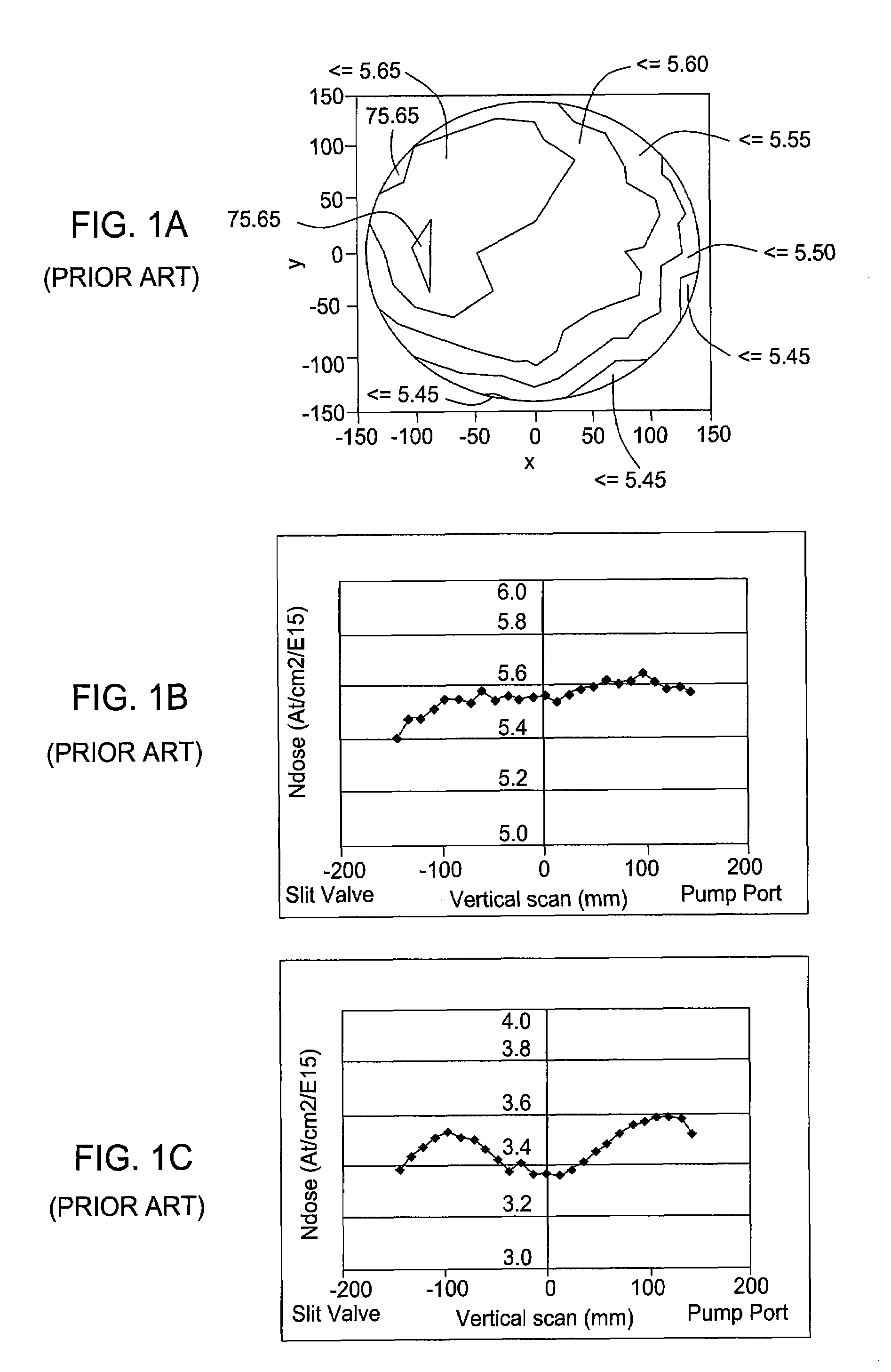
a technology of inductively coupled plasma and substrate, applied in the direction of plasma technique, chemical vapor deposition coating, coating, etc., can solve the problem of becoming more difficult to maintain a uniform plasma ion density across the entire wafer surface, and achieve the effect of reducing asymmetry

Inactive Publication Date: 2009-06-25
APPLIED MATERIALS INC
View PDF27 Cites 24 Cited by
  • Summary
  • Abstract
  • Description
  • Claims
  • Application Information

AI Technical Summary

Benefits of technology

[0015]Yet another embodiment of the present invention provides a method for adjusting process uniformity in a plasma reactor comprising positioning a substrate on a pedestal assembly disposed in a process volume of a chamber body, wherein the plasma reactor comprises a gas supply assembly having at least two independently gas passages, each configured to direct a process gas to a

Problems solved by technology

However, it becomes more difficult to maintain a uniform plasma io

Method used


Image

  • Apparatus and method for processing a substrate using inductively coupled plasma technology
  • Apparatus and method for processing a substrate using inductively coupled plasma technology
  • Apparatus and method for processing a substrate using inductively coupled plasma technology

Examples


Embodiment Construction

[0029]The present invention generally provides apparatus and method for processing a semiconductor substrate using inductively coupled plasma. Embodiments of the present invention provide inductively coupled plasma reactors having features provides improved uniformity. Particularly, the inductively coupled plasma reactors of the present invention comprises adjustable coils to reduce non-uniformity in the form of skew, a substrate assembly capable of adjusting edge performance, and an gas inject assembly having independently adjustable gas injects.

System Overview

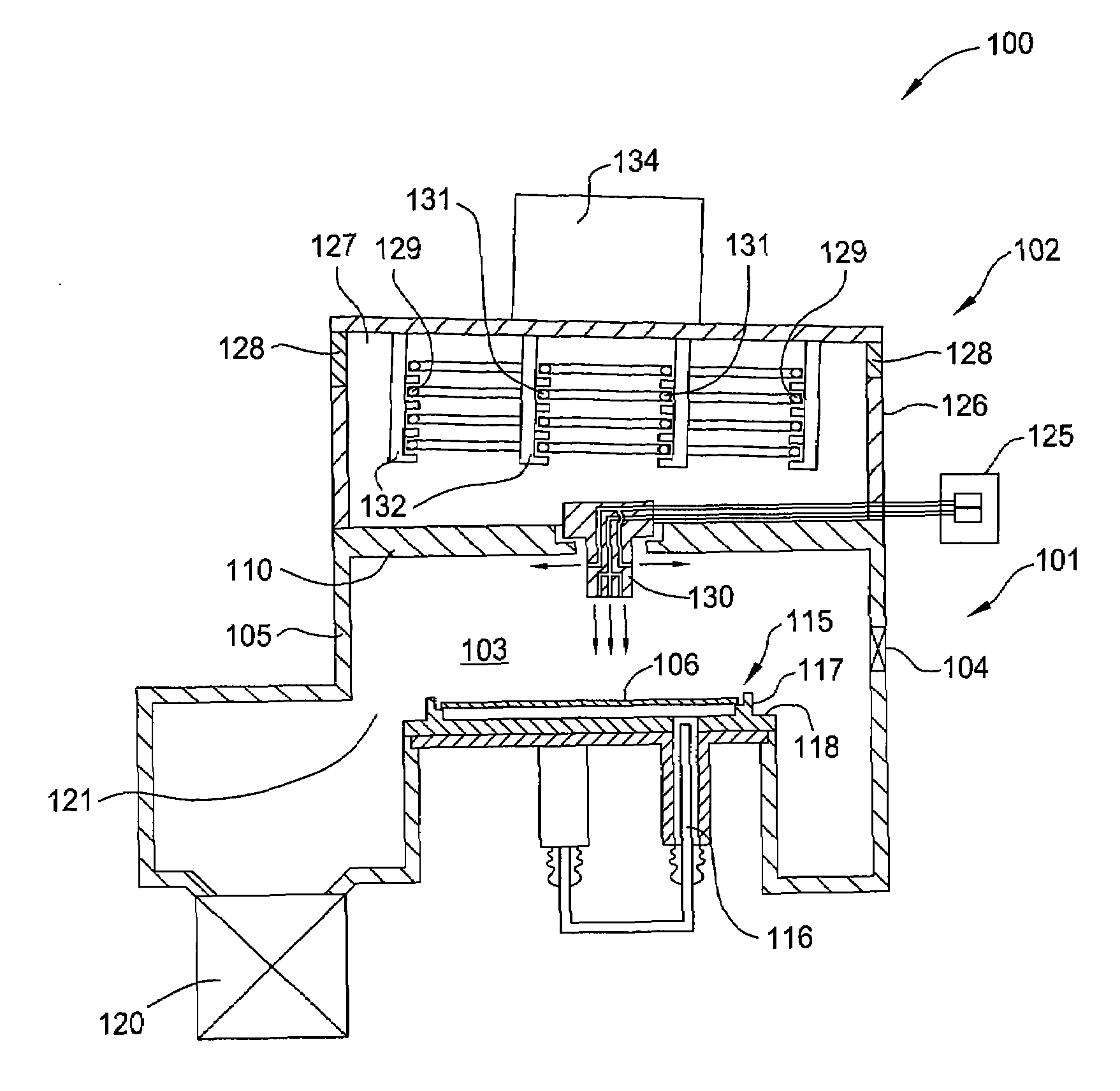
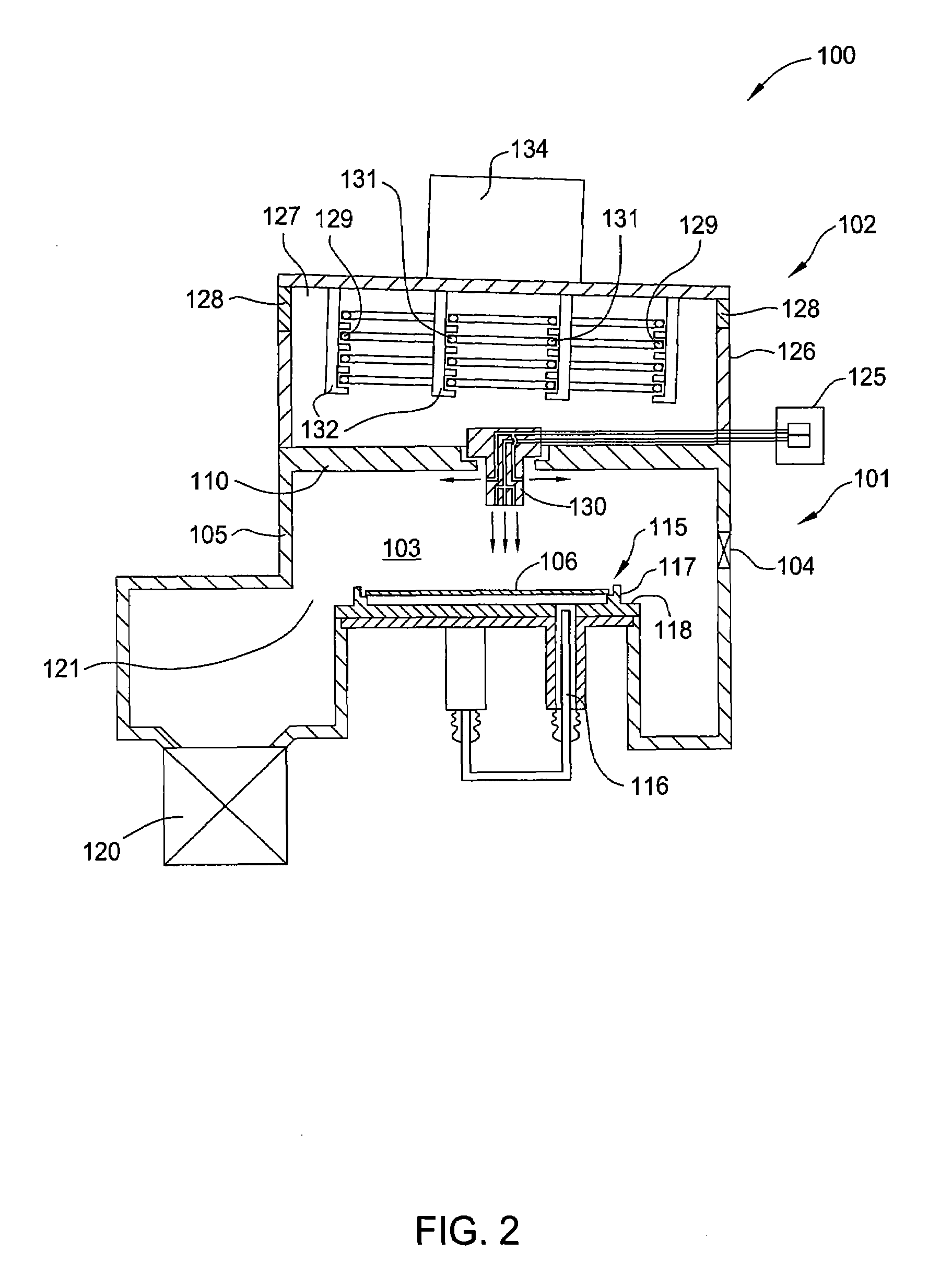
[0030]FIG. 2 schematically illustrates a sectional side view of a plasma reactor 100 in accordance with one embodiment of the present invention. The plasma reactor 100 generally comprises a reactor chamber 101 and an antenna assembly 102 positioned above the reactor chamber 101. The antenna assembly 102 is configured to generate inductively coupled plasma in the reactor chamber 101.

[0031]The reactor chamber 101 has a process ...


PUM

PropertyMeasurementUnit
Lengthaaaaaaaaaa
Lengthaaaaaaaaaa
Thicknessaaaaaaaaaa

Abstract

The present invention generally provides apparatus and methods for processing a semiconductor substrate. Particularly, the present invention provides an inductively coupled plasma reactor having improved process uniformity. One embodiment of the present invention provides an apparatus for processing a substrate comprising a chamber body defining a process volume configured to process the substrate therein, an adjustable coil assembly coupled to the chamber body outside the process volume, a supporting pedestal disposed in the process volume and configured to support the substrate therein, and a gas injection assembly configured to supply a process gas towards a first process zone and a second process zone independently.

Description

BACKGROUND OF THE INVENTION[0001]1. Field of the Invention[0002]Embodiments of the present invention generally relate to method and apparatus for processing a semiconductor substrate. More particularly, embodiments of the present invention provide method and apparatus for processing a semiconductor substrate using inductively coupled plasma technology with improved uniformity.[0003]2. Description of the Related Art[0004]Plasma reactors used to fabricate semiconductor microelectronic circuits can employ RF (radio frequency) inductively coupled fields to maintain a plasma formed from a processing gas. Conventional inductively coupled plasma reactors generally includes a vacuum chamber having a side wall and a ceiling, a workpiece support pedestal within the chamber and generally facing the ceiling, a gas inlet capable of supplying a process gas into the chamber, and one or more coil antennas overlying the ceiling. The one or more coil antennas are generally wound about an axis of symm...

Claims


Application Information

Patent Timeline
IPC IPC(8): H05H1/24C23C16/503
CPCH01J37/321H01J37/32174H01J37/3211
Inventor SWENBERG, JOHANES F.LIU, WEINGUYEN, HANH D.NGUYEN, SON T.CURTIS, ROGERBOTTINI, PHILIP A.MARK, MICHAEL J.GUARINI, THERESA KRAMERCHOI, WOONG
Owner APPLIED MATERIALS INC
Why Eureka
Try Eureka