Pad in Semicondcutor Device and Fabricating Method Thereof

a semiconductor device and semiconductor technology, applied in the field of semiconductor devices, can solve the problems of unnecessary parasitic capacitance generation and failure of integrated circuits, and achieve the effects of reducing the total parasitic capacitance components, minimizing design errors, and reducing the influence of parasitic factors

Inactive Publication Date: 2009-07-02
DSS TECH MANAGEMENT
View PDF3 Cites 13 Cited by
  • Summary
  • Abstract
  • Description
  • Claims
  • Application Information

AI Technical Summary

Benefits of technology

[0017]Accordingly, the present invention reduces total parasitic capacitance components by connecting MIM type capacitors in series together, preferably not overlapping with each other, thereby minimizing design error(s) attributed to the pad by reducing influence on parasitic factors generated from integrated circuit design.
[0018]The MIM capacitors formed by the present method have a series and / or spiral configuration, thereby generating less inductance and / or reducing capacitance attributed to the MIM capacitor serial connection, if necessary. Therefore, it is able to minimize capacitance attributed to resonance at a specific frequency.
[0019]Moreover, the present invention avoids affecting a neighboring pad or circuit without additional processing or additional structures, despite maintaining the above-mentioned effects, thereby reducing a cost.

Problems solved by technology

Since the above structure configures a series of MIM (metal-insulator-metal) capacitors, unnecessary parasitic capacitance is generated in designing an AC integrated circuit.
If the parasitic capacitance is not considered in designing an integrated circuit, the integrated circuit may malfunction.
However, the spiral inductor inserted to reduce the parasitic capacitance may affect a circuit adjacent to the inductor or a neighboring pad.

Method used


Image

  • Pad in Semicondcutor Device and Fabricating Method Thereof
  • Pad in Semicondcutor Device and Fabricating Method Thereof
  • Pad in Semicondcutor Device and Fabricating Method Thereof

Examples


Embodiment Construction

[0025]Reference will now be made in detail to preferred embodiments of the present invention, examples of which are illustrated in the accompanying drawings. Wherever possible, the same reference numbers will be used throughout the drawings to refer to the same or like parts.

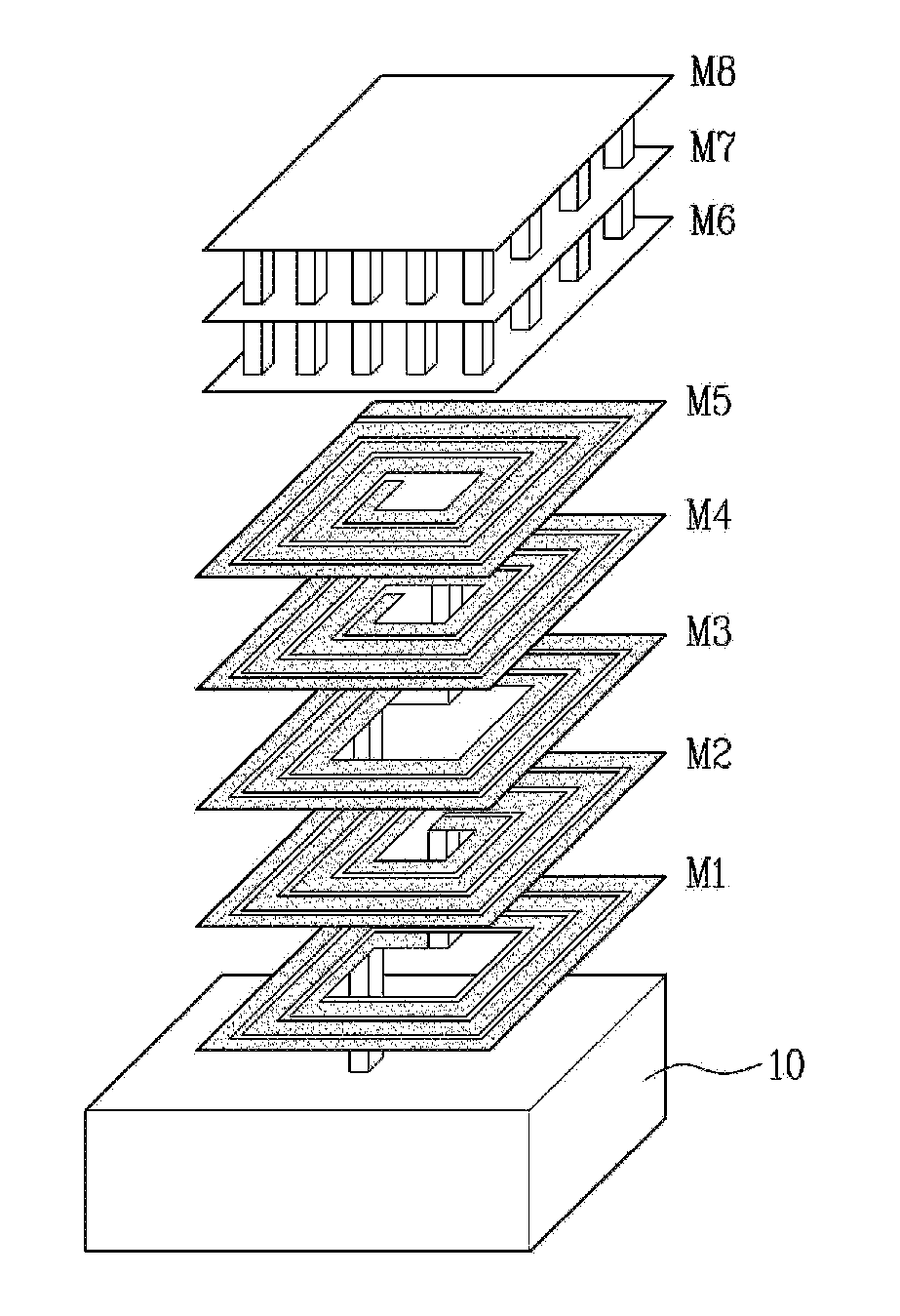
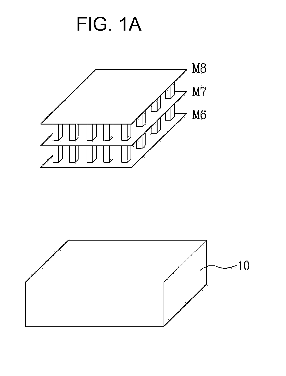
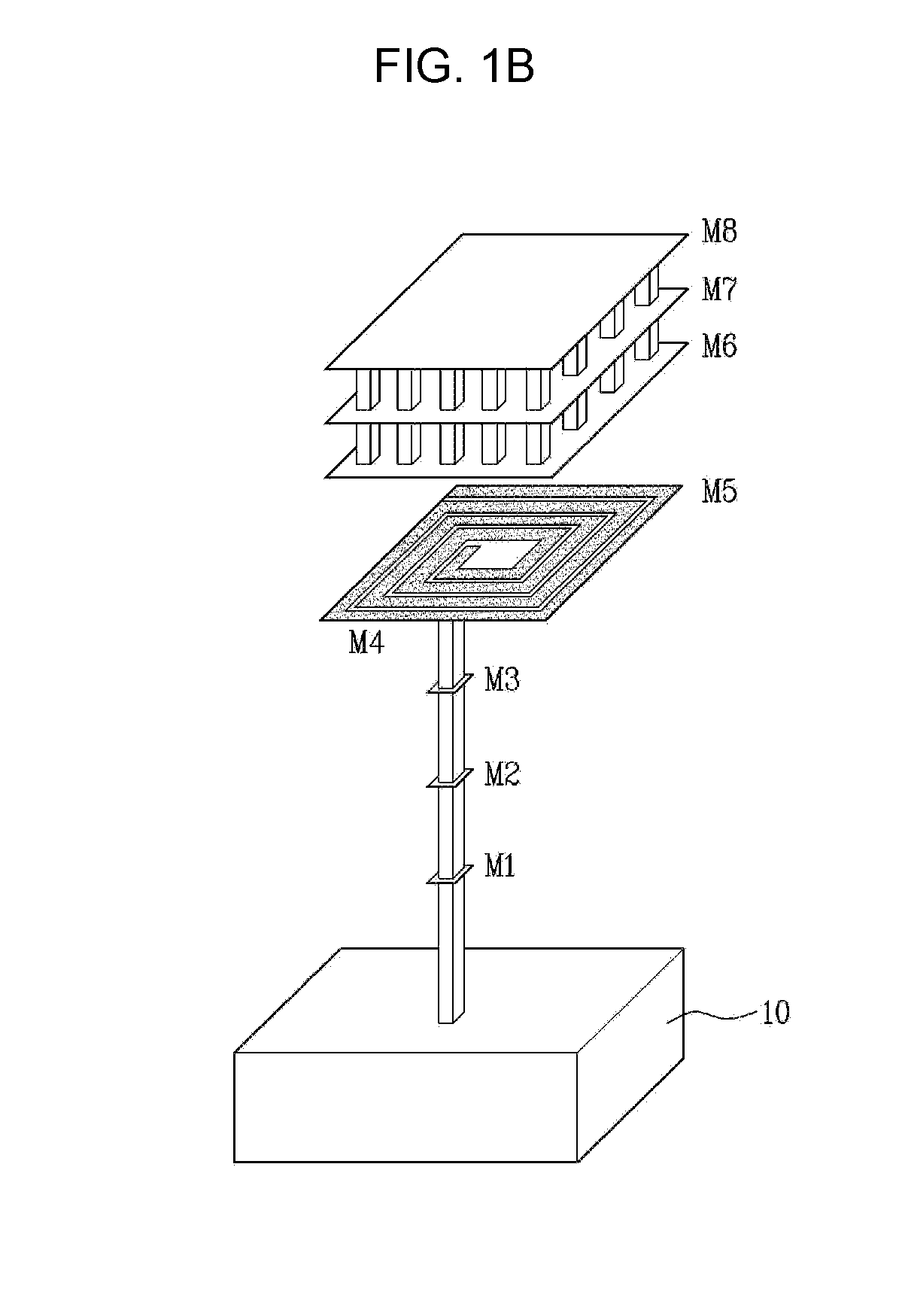
[0026]FIG. 2 is a layout of an exemplary pad in a semiconductor device according to embodiments of the present invention and FIG. 3 is a front diagram of the exemplary pad shown in FIG. 2.

[0027]An uppermost metal layer 100 can be provided, generally as a relatively large sheet, square or rectangle that may have dimensions on the order of 10-200 μm per side, preferably on the order of 40-120 μm per side. 1st to Nth intermediate metal layers are in sequence below the metal layer 100. In this case, N is a positive integer equal to or greater than 1, preferably≧2. When N≧2, a plurality of MIM capacitors may be formed in series and / or in parallel.

[0028]Referring to FIG. 2 and FIG. 3, if N=5, a fifth intermediate meta...


PUM

PropertyMeasurementUnit
areaaaaaaaaaaa
conductiveaaaaaaaaaa
dielectricaaaaaaaaaa

Abstract

A pad in a semiconductor device and fabricating method thereof are disclosed. The pad includes an uppermost metal layer first to Nth intermediate metal layers, wherein capacitors configured or formed by the uppermost metal layer and the first to Nth intermediate metal layers are serially connected. Accordingly, the pad reduces total parasitic capacitance components by connecting MIM type capacitors in series, and not necessarily overlapping with each other, thereby minimizing design errors attributed to the pad by reducing parasitic factors generated from the integrated circuit design. The pad may also minimize capacitance attributed to resonance at a specific frequency. Moreover, the pad avoids affecting an adjacent pad or circuit without additional processing, despite maintaining the above-mentioned effects, thereby reducing cost.

Description

[0001]This application claims the benefit of the Korean Patent Application No. 10-2007-0137173, filed on Dec. 26, 2007, which is hereby incorporated by reference as if fully set forth herein.BACKGROUND OF THE INVENTION[0002]1. Field of the Invention[0003]The present invention relates to a semiconductor device, and more particularly, to a pad in a semiconductor device and a fabricating method thereof.[0004]2. Discussion of the Related Art[0005]Generally, a pad is an element mandatory for MMIC (Micro-wave Monolithic Integrated Circuit) or RFIC (Radio Frequency Integrated Circuit) using semiconductor devices. A pad in a semiconductor device is necessary for signal input / output, for measuring characteristics of the device directly, and / or for wire bonding in the case of packaging a fabricated integrated circuit (IC). Namely, the semiconductor device pad plays a role in transferring a signal or supplying a power (or transferring a power) to or from the IC.[0006]A general pad in a semicon...

Claims


Application Information

Patent Timeline
Patent Type & Authority Applications(United States)
IPC IPC(8): H01G4/30H01L21/20
CPCH01G4/30H01L2924/01033H01L23/5223H01L23/5227H01L24/03H01L24/05H01L2224/05093H01L2224/05096H01L2924/01013H01L2924/01014H01L2924/01015H01L2924/01022H01L2924/01029H01L2924/01047H01L2924/0105H01L2924/01074H01L2924/05042H01L2924/14H01L2924/1423H01L2924/19041H01L2924/19042H01L2924/30105H01L2924/30107H01L2924/01005H01G4/38H01L21/3205H01L21/768H01L23/48
Inventor KIM, SUNG SU
Owner DSS TECH MANAGEMENT
Why Eureka
Try Eureka