Semiconductor memory cell and semiconductor memory array using the same

Inactive Publication Date: 2009-07-09
PANASONIC CORP
View PDF13 Cites 17 Cited by
  • Summary
  • Abstract
  • Description
  • Claims
  • Application Information

AI Technical Summary

Benefits of technology

[0021]In this configuration, since the channel region made of the semiconductor film is formed over the back-gate electrode which is larger than the channel region, the channel region is composed of the smooth semiconductor film having no steps. This allows the semiconductor memory cell to have stable characteristics.
[0022]In addition, when semiconductor memory cells thus configured are arranged in an array to form a semiconductor memory array, the back-gate electrode can also be used as a common electrode in the semiconductor memory cells. It is thus possible to achieve a high-density semiconductor memory array.
[0023]In one embodiment, a part of the ferroelectric film located under the first gate electrode is polarized in a first direction, and a part of the ferroelectric film located under the second gate electrode is polarized in a second direction which is opposite to the first direction, thereby resetting the semiconductor memory cell so that a part of the channel located under the first gate electrode has a low resistance and a part of the channel located under the second gate electrode has a high resistance.
[0024]In another embodiment, a pre

Problems solved by technology

Nevertheless, when a MFSFET serving as a memory element and a MISFET serving as a selection switch are placed side by side in order to prevent write di

Method used


Image

  • Semiconductor memory cell and semiconductor memory array using the same
  • Semiconductor memory cell and semiconductor memory array using the same
  • Semiconductor memory cell and semiconductor memory array using the same

Examples


Example

FIRST EMBODIMENT

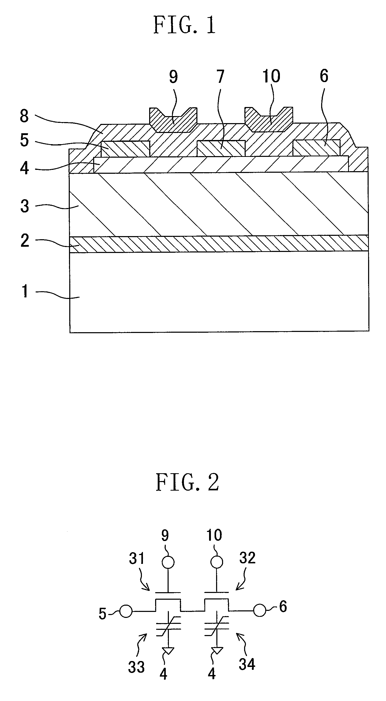
[0046]FIG. 1 is a cross-sectional view schematically illustrating the configuration of a semiconductor memory cell according to a first embodiment of the present invention, and FIG. 2 illustrates an equivalent circuit thereof.

[0047]As shown in FIG. 2, the semiconductor memory cell of this embodiment has a configuration in which a memory element composed of a first field effect transistor (which will be hereinafter referred to as a “first FET”) 31 and a selection switch composed of a second field effect transistor (which will be hereinafter referred to as a “second FET”) 32 are connected in series.

[0048]Also, as shown in FIG. 1, a semiconductor film 4 and a dielectric film 8 stacked over a substrate 1 form a common channel and a common gate insulating film in the first and second FETs 31 and 32. On the dielectric film 8, a first gate electrode 9 of the first FET 31 and a second gate electrode 10 of the second FET 32 are formed. On the semiconductor film 4, a drain ele...

Example

SECOND EMBODIMENT

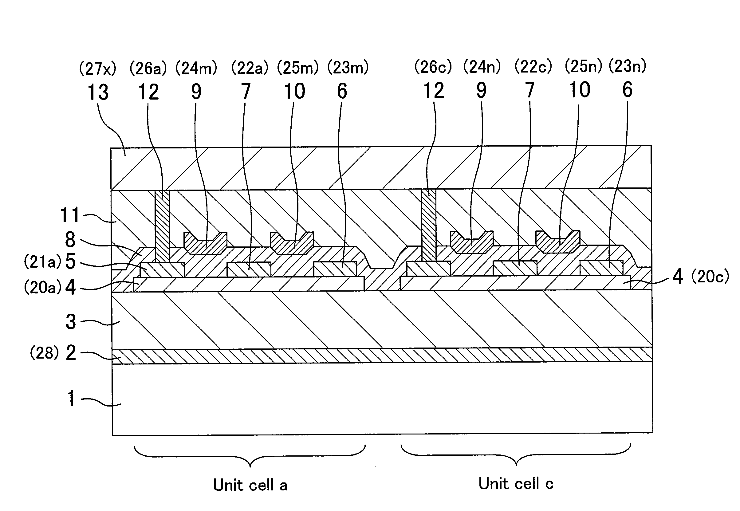
[0076]In the first embodiment, the basic configuration and operation of the semiconductor memory cell according to the present invention have been described. In this embodiment, a semiconductor memory array in which semiconductor memory cells of the present invention are arranged in an array will be described.

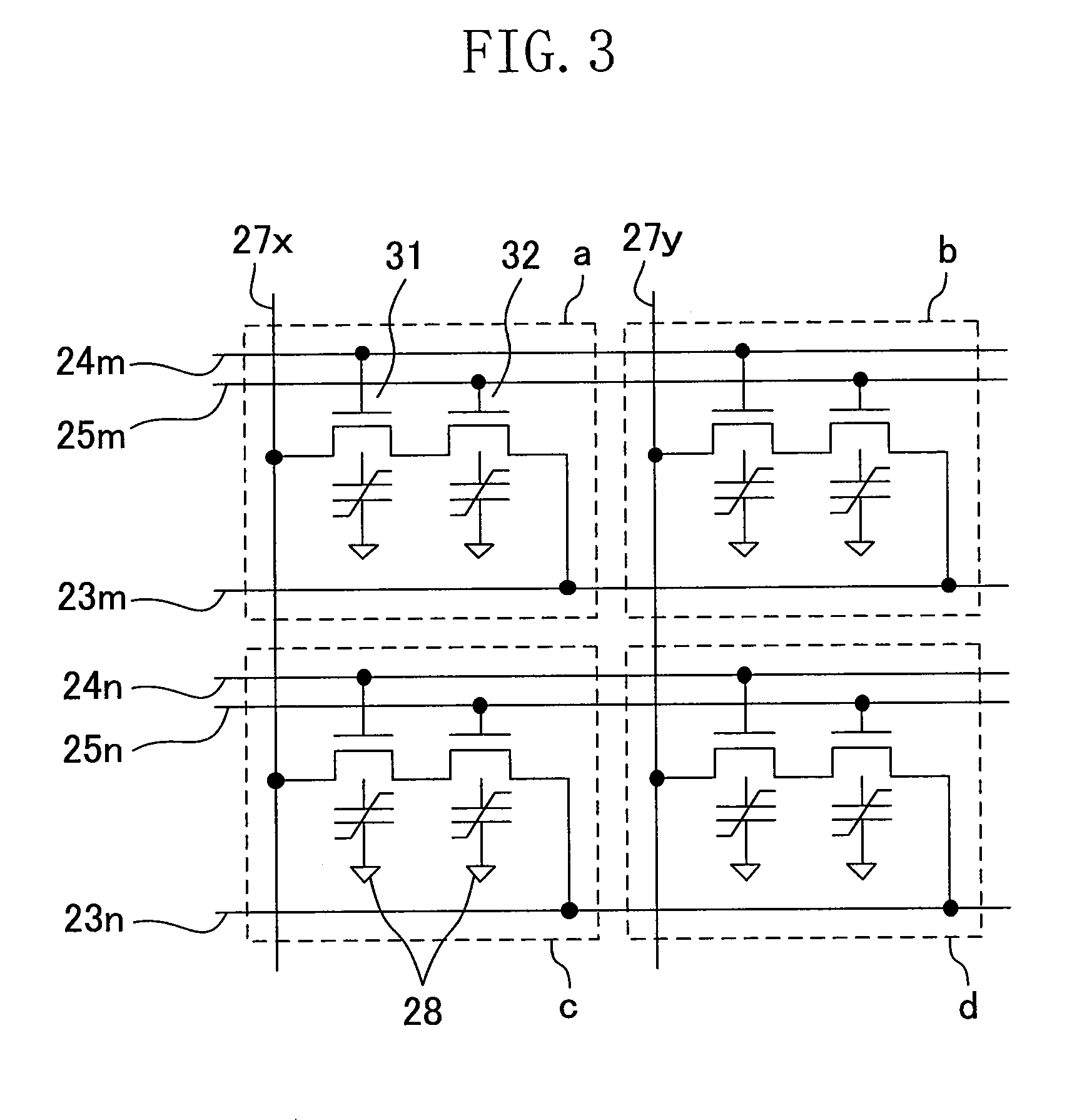
[0077]FIG. 3 illustrates the circuit configuration of the semiconductor memory array according to this embodiment. FIG. 4 is a plan view illustrating a layout when the semiconductor memory array is formed on a semiconductor substrate. FIG. 5 is a cross-sectional view taken along the line V-V in FIG. 4 and illustrating the configuration of the semiconductor memory array.

[0078]In this embodiment, a semiconductor memory array having two rows and two columns will be described by way of example.

[0079]As shown in FIG. 3, in semiconductor memory cells (unit cells) a to d, first gate electrodes in each row are connected with a first word line 24m or 24n. Second gate el...


PUM


Abstract

A memory element including a first FET, and a selection switch including a second FET are connected in series, and a semiconductor film and a dielectric film stacked over a substrate form a common channel and a common gate insulating film in the first and second FETs. A first gate electrode of the first FET and a second gate electrode of the second FET are formed on the dielectric film, and a drain electrode and a source electrode are formed on the semiconductor film. Under the semiconductor film, a back-gate electrode is formed with a ferroelectric film interposed therebetween, and the ends of the semiconductor film that forms the channel are located inwardly of the ends of the back-gate electrode.

Description

BACKGROUND OF THE INVENTION[0001]1. Field of the Invention[0002]The present invention relates to a nonvolatile semiconductor memory cell utilizing channel resistance modulation in a semiconductor layer occurring due to remanent polarization of a ferroelectric material, and also relates to a semiconductor memory array using the nonvolatile semiconductor memory cell.[0003]2. Description of the Related Art[0004]Nonvolatile memories using ferroelectric materials are broadly divided into two types: a capacitor-type and a field effect transistor (FET)-type having a gate insulating film made of a ferroelectric film.[0005]The capacitor-type nonvolatile ferroelectric memories, which are similar in structure to dynamic random access memories (DRAMs), hold charges in a ferroelectric capacitor therein and identify whether binary data is 0 or 1 according to the direction of polarization of the ferroelectric material. The polarization accumulated in the ferroelectric capacitor is coupled to charg...

Claims


Application Information

Patent Timeline
IPC IPC(8): H01L29/78
CPCG11C11/22H01L27/1159G11C11/221H10B51/30
Inventor KATO, YOSHIHISA
Owner PANASONIC CORP
Why Eureka
Try Eureka