Heat treatment apparatus for heating substrate by exposing substrate to flash light

Inactive Publication Date: 2009-07-09
DAINIPPON SCREEN MTG CO LTD
View PDF6 Cites 52 Cited by
  • Summary
  • Abstract
  • Description
  • Claims
  • Application Information

AI Technical Summary

Benefits of technology

[0017]This suppresses changes in the temperature of the device formation region due to the contact with the support pins to prevent the treatment failure of the device f

Problems solved by technology

The occurrence of such a phenomenon causes the depth of the junction to exceed a required level, giving rise to an apprehension about a hindrance to good device formation.
Also, it has turned out that flash light emitted in an extremely short time of several milliseconds or less can achieve a selective temperature rise only near the surface of the semiconductor wafer.
A heat treatment apparatus employing such a xenon flash lamp, which momentarily exposes the semiconductor wafer

Method used


Image

  • Heat treatment apparatus for heating substrate by exposing substrate to flash light
  • Heat treatment apparatus for heating substrate by exposing substrate to flash light
  • Heat treatment apparatus for heating substrate by exposing substrate to flash light

Examples


Embodiment Construction

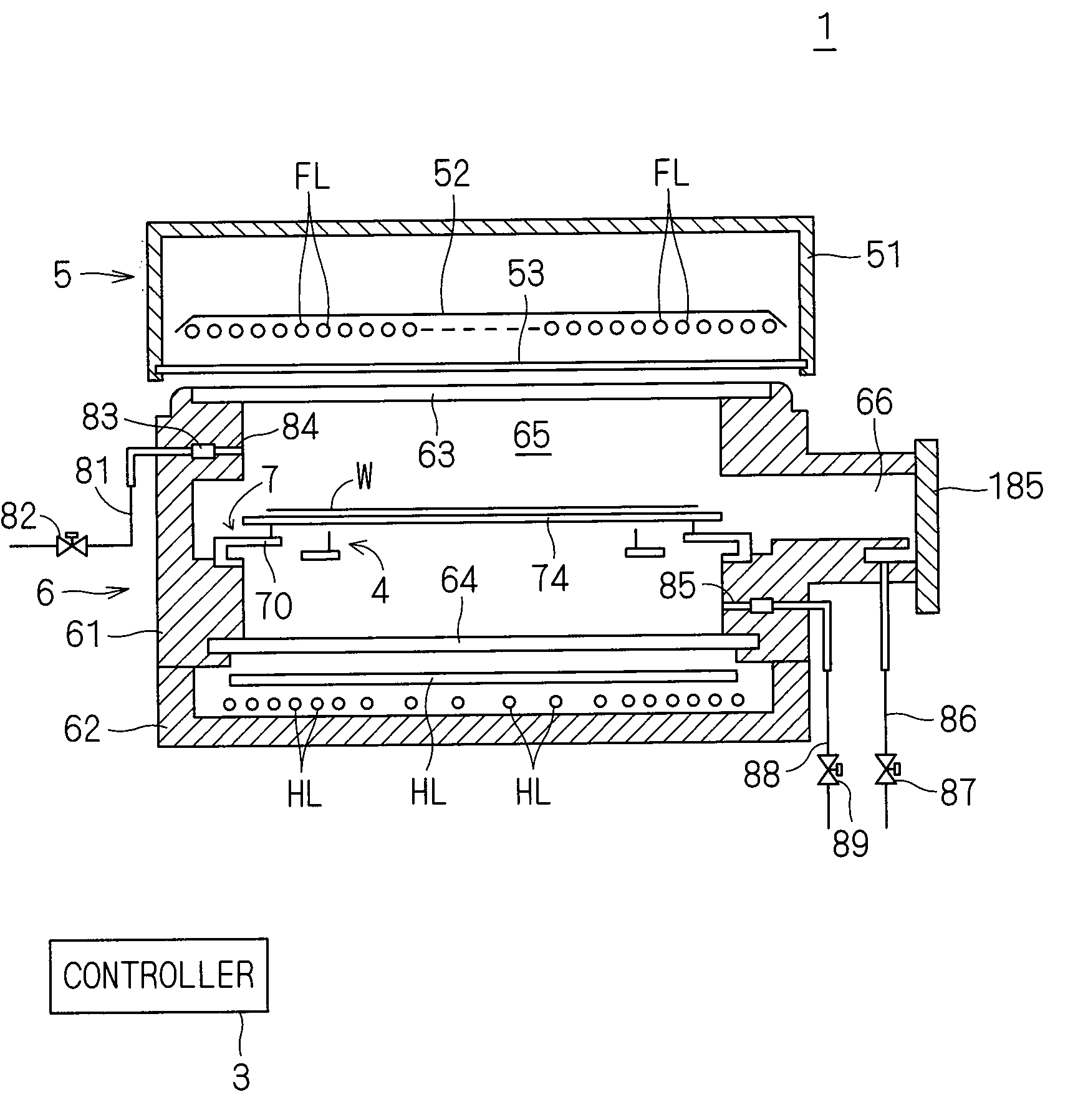
[0027]A preferred embodiment according to the present invention will now be described in detail with reference to the drawings.

[0028]First, the overall construction of a heat treatment apparatus according to the present invention will be outlined. FIG. 1 is a side sectional view showing the construction of a heat treatment apparatus 1 according to the present invention. The heat treatment apparatus 1 according to the preferred embodiment of the present invention is a flash lamp annealer for exposing a disc-shaped semiconductor wafer W having a diameter of 300 mm and serving as a substrate to flash light to heat the semiconductor wafer W.

[0029]The heat treatment apparatus 1 includes a chamber 6 for receiving a semiconductor wafer W therein, and a lamp house 5 containing a plurality of flash lamps FL. The heat treatment apparatus 1 further includes a controller 3 for controlling operating mechanisms provided in the chamber 6 and the lamp house 5 to cause the operating mechanisms to he...


PUM


Abstract

A semiconductor wafer to be treated is placed in a horizontal position on a holding plate held by a susceptor. Six bumps are mounted upright on the upper surface of the holding plate. The semiconductor wafer is supported by the six bumps in point contacting relationship, and is held at a distance ranging from 0.5 mm to 3 mm from the upper surface of the holding plate. Light is directed from halogen lamps onto the semiconductor wafer held by the holding plate to preheat the substrate until the temperature of the semiconductor wafer is increased up to a predetermined temperature. Thereafter, flash light is directed from flash lamps onto the semiconductor wafer. A thin gas layer lying between the back surface of the semiconductor wafer and the upper surface of the holding plate acts as a resistance to suppress the motion of the semiconductor wafer, thereby preventing a crack in the semiconductor wafer.

Description

BACKGROUND OF THE INVENTION[0001]1. Field of the Invention[0002]The present invention relates to a heat treatment apparatus for heating a substrate including a semiconductor wafer, a glass substrate and the like by exposing the substrate to flash light.[0003]2. Description of the Background Art[0004]Conventionally, a lamp annealer employing a halogen lamp has been typically used in the step of activating ions in a semiconductor wafer after ion implantation. Such a lamp annealer carries out the activation of ions in the semiconductor wafer by heating (or annealing) the semiconductor wafer up to a temperature of, for example, about 1000° C. to about 1100° C. Such a heat treatment apparatus utilizes the energy of light emitted from the halogen lamp to raise the temperature of a substrate at a rate of about hundreds of degrees per second.[0005]In recent years, with the increasing degree of integration of semiconductor devices, it has been desired to provide a shallower junction as the g...

Claims


Application Information

Patent Timeline
IPC IPC(8): A21B2/00
CPCH01L21/6875H01L21/67115
Inventor KOBAYASHI, IPPEI
Owner DAINIPPON SCREEN MTG CO LTD
Why Eureka
Try Eureka