Antireflection structure formation method and antireflection structure

Inactive Publication Date: 2009-07-09
KK TOSHIBA
View PDF7 Cites 34 Cited by
  • Summary
  • Abstract
  • Description
  • Claims
  • Application Information

AI Technical Summary

Benefits of technology

[0056]The present invention in one embodiment provides a formation method by which an antireflection structure excellent in antireflection functions can be produc

Problems solved by technology

However, although fine patterns can be formed very precisely, these fabrication technologies are not suitable for industrial applications because they need expensive apparatuses and give low throughput.
However, in the process, the selective etching ratio between the particles and the substrate is too large to form projections having high antireflection functions.
However, although projections can be almost obtained, this etching process comprises complicated procedures since the etching gas mu

Method used


Image

  • Antireflection structure formation method and antireflection structure
  • Antireflection structure formation method and antireflection structure
  • Antireflection structure formation method and antireflection structure

Examples


example 1

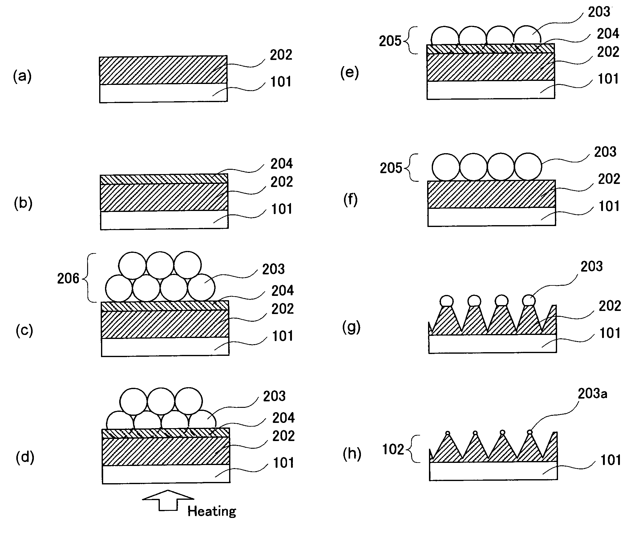
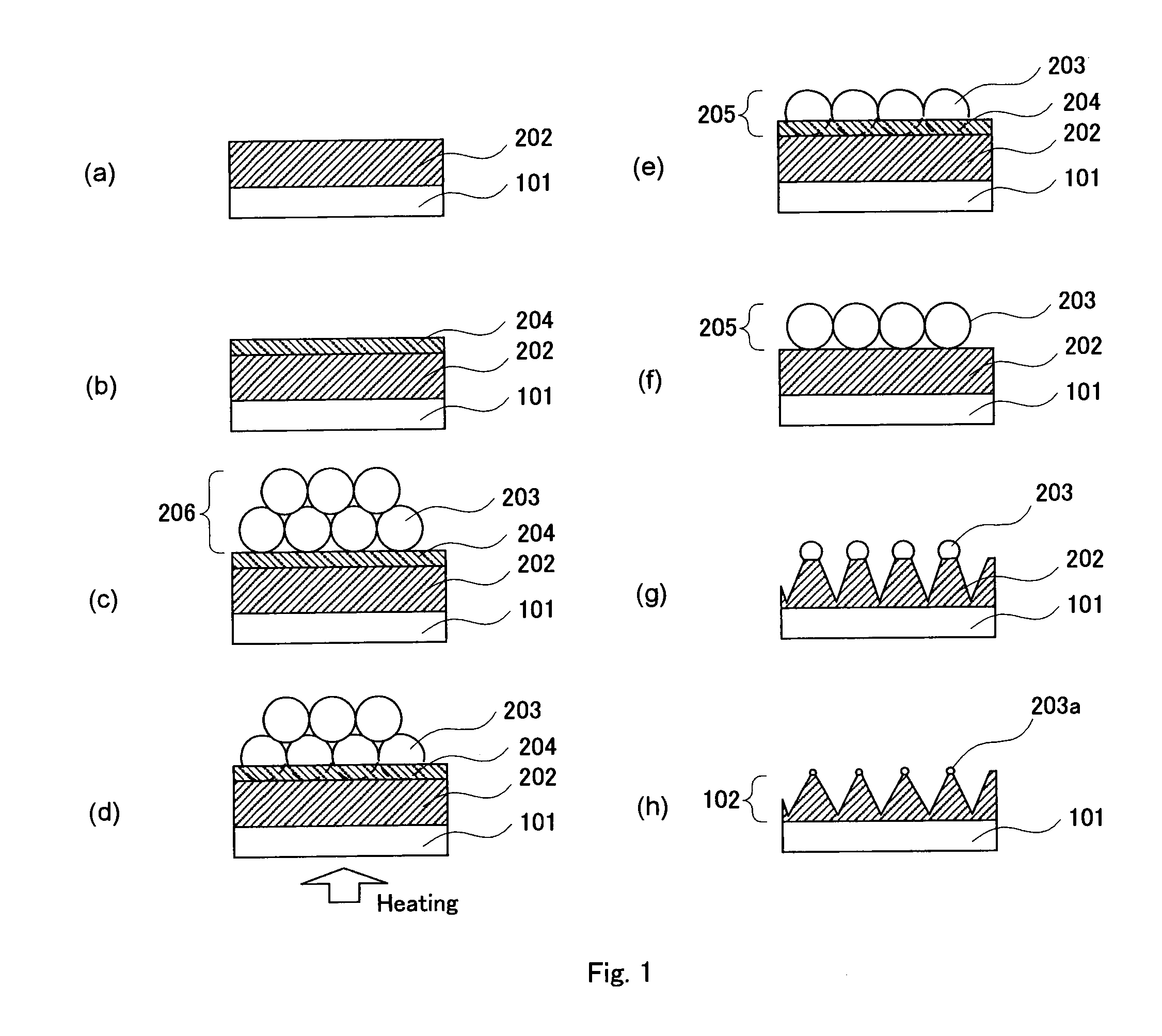
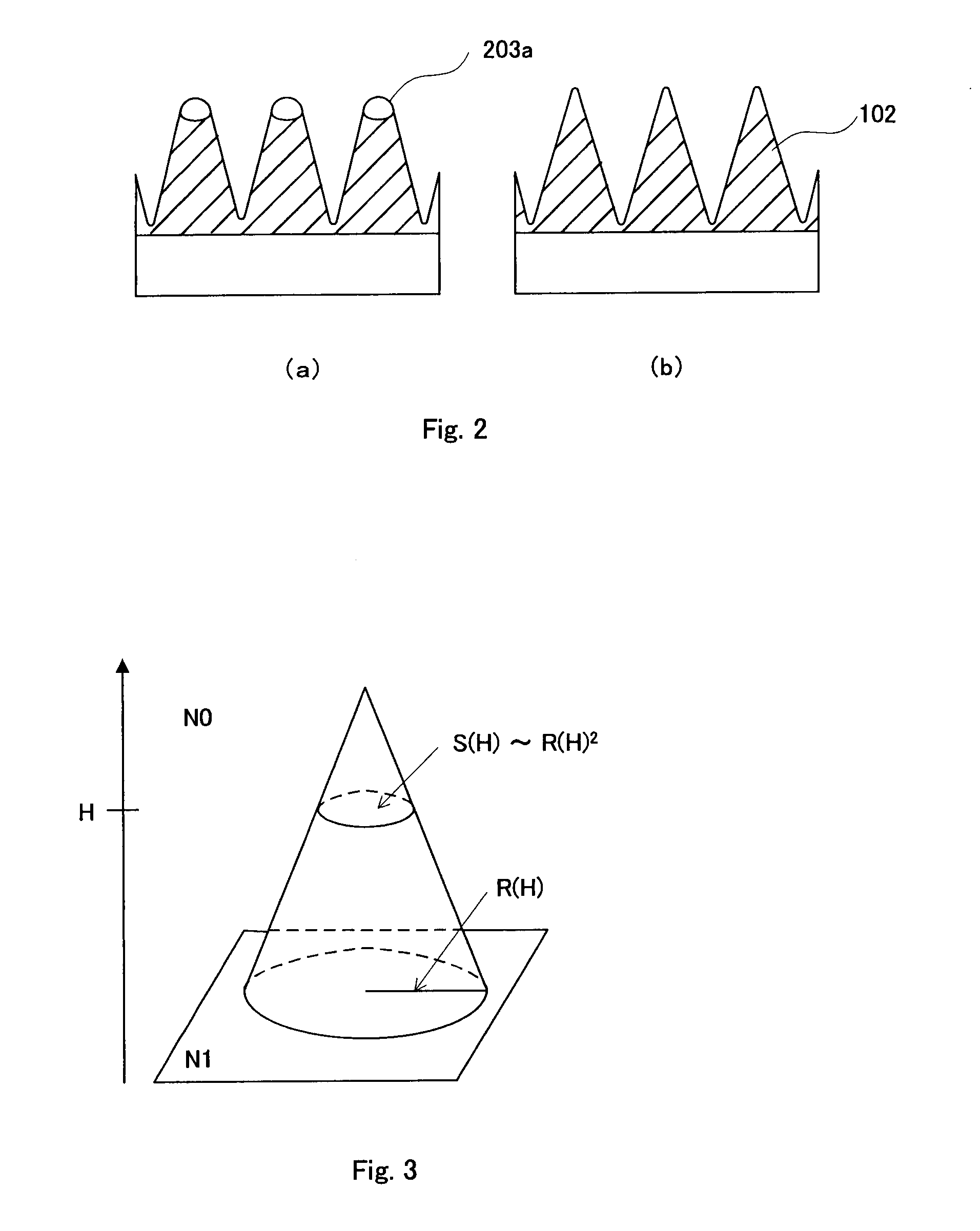
[0102]As a substrate, a 4-inch quartz substrate (synthesized quartz glass AQ™, manufactured by Asahi Glass Co., Ltd.) was prepared. On the substrate, spin-on glass material (hereinafter, often referred to as “SOG material”) (OCD-T7™, manufactured by Tokyo Ohka Kogyo Co., Ltd.), as a material for the base layer from which the antireflection structure was to be formed, was spin-coated at 2000 rpm for 40 seconds, and then baked on a hot-plate at 110° C. for 90 seconds. The substrate was annealed in a N2 oven at 300° C. for 35 minutes. The thickness of the SOG membrane thus formed was observed by scanning electron microscope (hereinafter, often referred to as “SEM”), and found to be 450 nm. Further, a resist for half-micron pattern (THMR-ip3250™, manufactured by Tokyo Ohka Kogyo Co., Ltd.), as a material for the particle-trap layer, was spin-coated at 2000 rpm for 35 seconds, and then baked on a hot-plate at 110° C. for 90 seconds. The thickness of the particle-trap layer thus formed wa...

example 2

[0105]As a substrate, a 6-inch Si substrate (manufactured by SUMCO Corporation) was prepared. The procedure of Example 1 was then repeated to form an antireflection structure comprising 350 nm-high SOG projections arranged at the interval of 210 nm on the 6-inch Si substrate. The obtained substrate was washed with water for 10 minutes, and dried on a hot-plate at 100° C. The silica particles on the tips of the projections were reacted with the SOG interface during the etching process, and thereby fixed so firmly that they did not come from the tips in washing.

[0106]The substrate after washed was then used as a master plate to form a nanoimprint stamper in the following manner. First, an electro-conductive membrane of Ni was formed on the substrate by a sputtering process. The sputtering process was carried out in a chamber which was beforehand evacuated to 8×10⁻³ Pa and then into which argon gas was introduced until the inner pressure reached 1 Pa. While pure nickel metal was used a...

example 3

[0111]As a substrate, a 6-inch Si substrate (manufactured by SUMCO Corporation) was prepared. After a resist for half-micron pattern (THMR-ip3250™, manufactured by Tokyo Ohka Kogyo Co., Ltd.) was diluted with ethyl lactate to 30%, the obtained solution was spin-coated on the Si substrate at 2000 rpm for 40 seconds and then baked on a hot-plate at 100° C. for 90 seconds. The substrate was further annealed in a N2 oven at 250° C. for 1 hour to harden the resist and thereby to form a resist layer (base layer). The thickness of the resist layer was measured with a stylus profilometer (Tallystep™, manufactured by Taylor Hobson K.K.) and found to be 400 nm. Successively, a 55 nm-thick PMMA membrane was formed thereon as the particle-trap layer. The surface of the particle-trap layer was then made hydrophilic by mean of parallel plate etching system (DEM-451™, manufactured by Canon ANELVA Corporation) under the conditions that: the etching gas was O2, the flowing amount was 30 sccm, the pr...


PUM

PropertyMeasurementUnit
Temperatureaaaaaaaaaa
Fractionaaaaaaaaaa

Abstract

The present invention provides such a formation method that an antireflection structure having excellent antireflection functions can be formed in a large area and at small cost. Further, the present invention also provides an antireflection structure formed by that method. In the formation method, a base layer and particles placed thereon are subjected to an etching process. The particles on the base layer serve as an etching mask in the process, and hence they are more durable against etching than the base layer. The etching rate ratio of the base layer to the particles is more than 1 but not more than 5. The etching process is stopped before the particles disappear. It is also possible to produce an antireflection structure by nanoimprinting method employing a stamper. The stamper is formed by use of a master plate produced according to the above formation method.

Description

CROSS-REFERENCE TO RELATED APPLICATION[0001]This application is based upon and claims the benefit of priority from the prior Japanese Patent Application No. 59 / 2008, filed on Jan. 4, 2008; the entire contents of which are incorporated herein by reference.BACKGROUND OF THE INVENTION[0002]1. Field of the Invention[0003]The present invention relates to an antireflection structure formation method and an antireflection structure.[0004]2. Background Art[0005]According as ultrafine micro-fabrication technologies used in LSI production processes and micro-machining processes have been developed recently, it has become possible to produce sub-wavelength gratings, which have periods shorter than the wavelength of light and which can be processed in nanometer scale. For example, as one of the sub-wavelength gratings, there is proposed a non-reflective periodic structure (see, Hiroshi Toyota, Kogaku (Japanese Journal of Optics [in Japanese]), Optical society of Japan, vol. 32 (2003), pp. 489)....

Claims


Application Information

Patent Timeline
IPC IPC(8): B05D5/02B05C19/00G02B1/11B32B7/02G02B1/02G02B1/118
CPCC03C15/00C03C17/007C03C2217/42Y10T428/24421C03C2218/34C03C2218/355G02B1/118C03C2217/77B81C1/0046C03C17/28
Inventor NAKANISHI, TSUTOMUFUJIMOTO, AKIRAASAKAWA, KOJIOKINO, TAKESHISUGIMURA, SHINOBU
Owner KK TOSHIBA
Why Eureka
Try Eureka