
Method of making circuitized substrates having film resistors as part thereof

Inactive Publication Date: 2009-07-16
I3 ELECTRONICS
View PDF25 Cites 22 Cited by
  • Summary
  • Abstract
  • Description
  • Claims
  • Application Information

AI Technical Summary

Benefits of technology

[0044]It is still another object to provide such a method which may be accomplished in a relatively facile manner and at relatively low costs in comparison to many known processes.

Problems solved by technology

This method has been found to be costly and time consuming in manufacturing hybrid film circuits because of the need for two or more different resistor compositions.
Such resistors are thus relatively expensive to produce and to position on the surface of a substrate layer (e.g., dielectric) to be connected to the selected parts of the circuit.
That is, precisely forming such resistors on selected locations of high density circuits with exacting resistor values is considered difficult when forming such high density circuit patterns as are so often required in many of today's micro-miniature circuit products.
This method, however, may distort the electrical field around the slice cut and produce undesirable variations in the impedance of the resistor at higher signal frequencies.
Known discrete passive devices, such as capacitors, resistors, inductors, and the like, typically occupy a relatively high percentage of the exterior surface area of the completed multilayered substrate product, which is undesirable from a future design aspect because of the aforementioned need for increased miniaturization.
Although the pre-fired and ground dielectric formulations produced by solid phase reactions are acceptable for many electrical applications, these suffer from several disadvantages.
First, the milling step may serve as a source of contaminants, which can adversely affect electrical properties.
Consequently, films produced using these powders are limited to thicknesses greater than the size of the largest particle.
Thirdly, powder suspensions or composites produced using pre-fired ground ceramic powders must be used immediately after dispersion, due to the high sedimentation rates associated with large particles.
It is thus clear that methods of making PCBs which rely on the advantageous features of using nano-powders as part of the circuitized substrate's internal components or the like may possess various undesirable aspects which are detrimental to providing a circuitized substrate with optimal functioning capabilities when it comes to internal resistance, capacitance or other electrical properties.
The thru-holes consume further space, especially when used in high density patterns such as up to 5,000 thru-holes per square inch of substrate surface area.
As is known, extremely close positioning of such thru-holes and signal lines and / or pads may result in discontinuities occurring therein, which will adversely affect the successful operation of the product, especially at high frequencies (which are also demanded in many products today).
These structures may result in signal degradation, particularly, as stated, when the signal lines and / or thru-holes are positioned in close proximity to one another.
Probing individual resistors on a work piece is time consuming and requires utilization of expensive capital equipment (a laser with an incorporated electrical test system).
This approach also becomes impractical from a cost standpoint when the number of individual resistors is large.
With circuitized substrates such as printed circuit boards and chip carriers requiring more and more discrete structures such as resistors, capacitors and the like as part thereof, the simultaneous probe and trim approach is now considered too costly.
Due to various processing limitations, the resistors comprising each stage vary slightly from their nominal value, which in turn upsets the current division.
The number of resistance measurements is limited by using non-measurement cuts, using non-sequential collinear cutting, using spot fan-out parallel cutting, and using a retrograde scanning technique for faster collinear cuts.

Method used


Image

  • Method of making circuitized substrates having film resistors as part thereof
  • Method of making circuitized substrates having film resistors as part thereof
  • Method of making circuitized substrates having film resistors as part thereof

Examples


Embodiment Construction

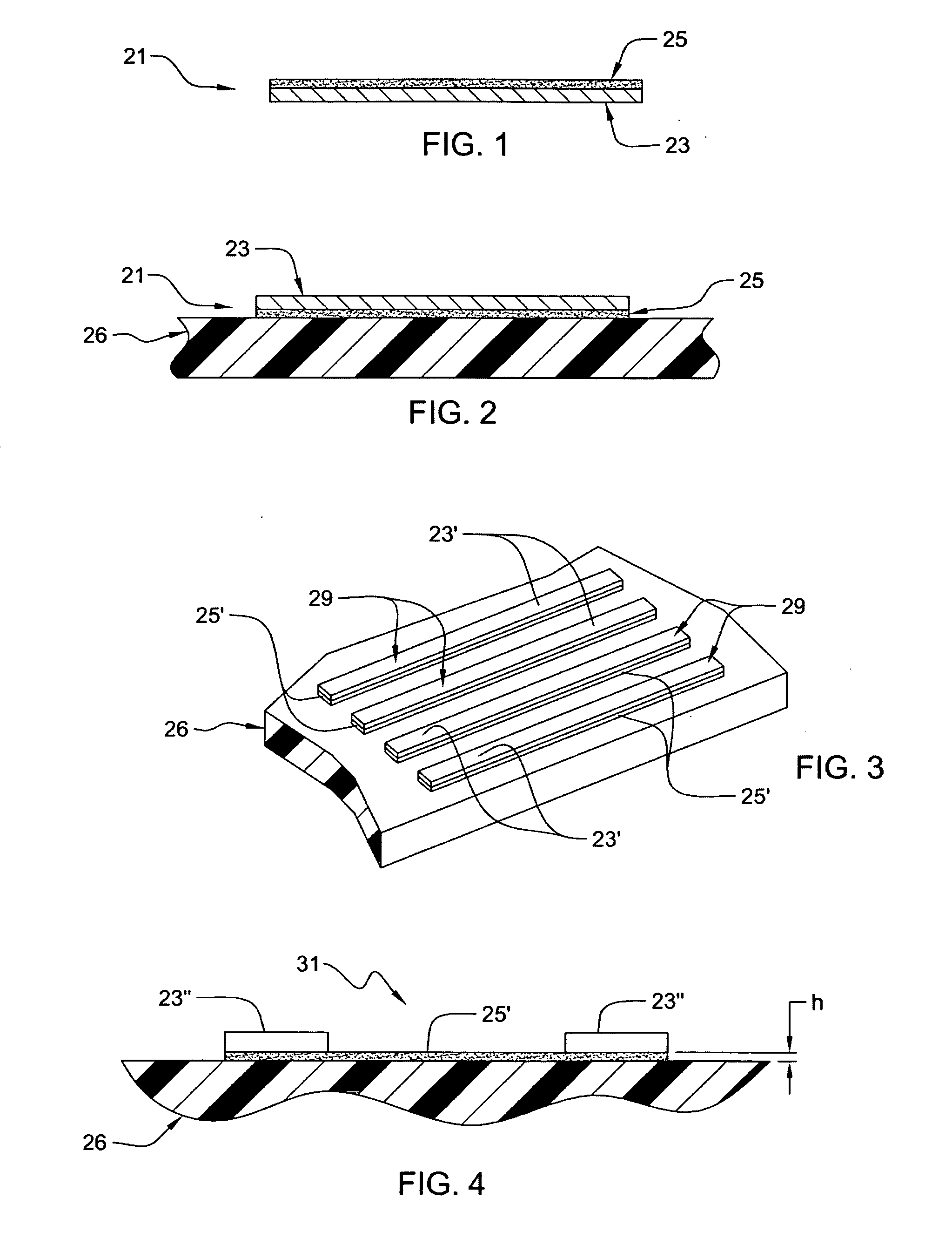
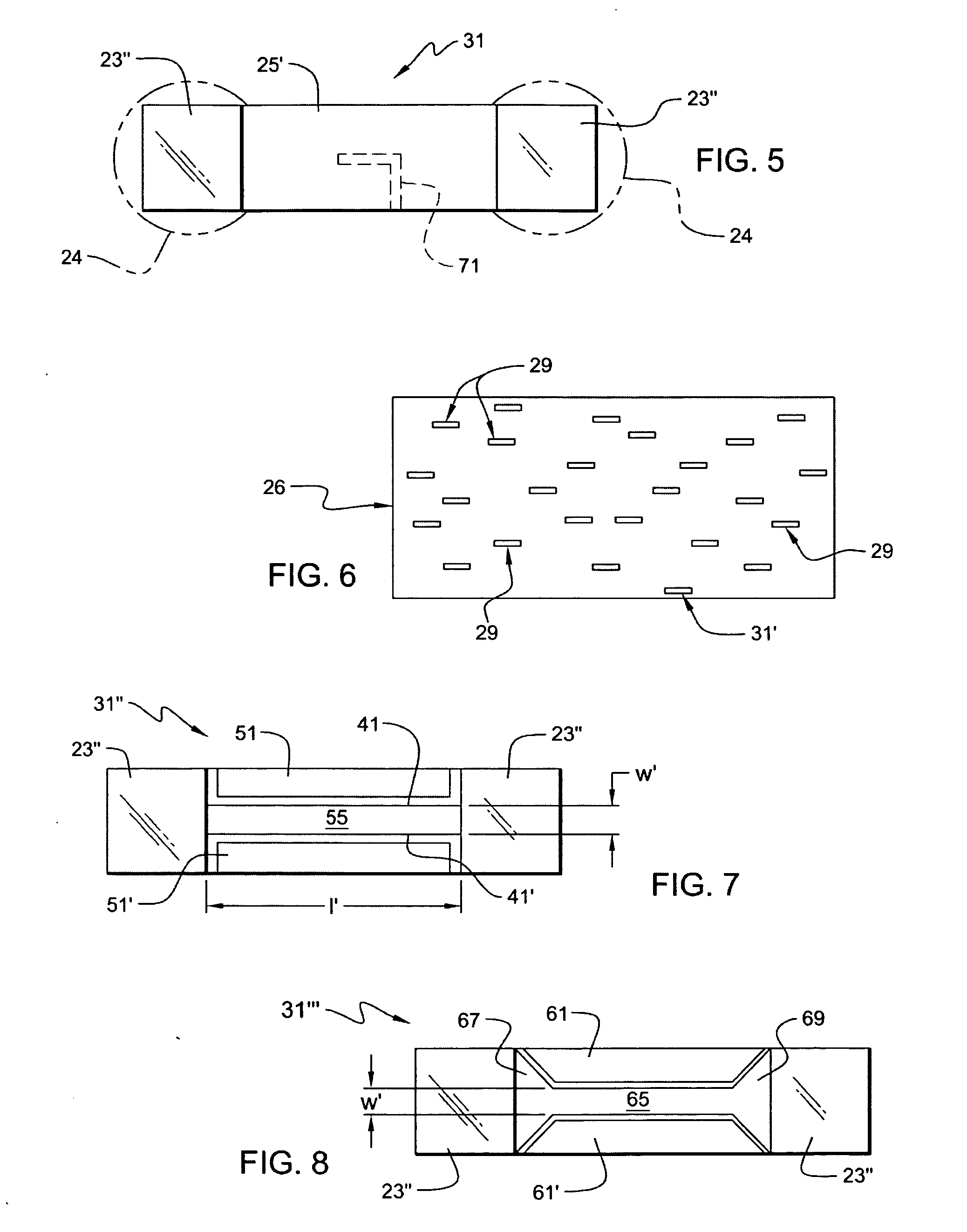
[0054]For a better understanding of the present invention, together with other and further objects, advantages and capabilities thereof, reference is made to the following disclosure and appended claims in connection with the above-described drawings. Like figure numbers are used from Figure to Figure to identify like elements in these drawings.

[0055]By the term “circuitized substrate” as used herein is meant to include substrates having at least one (and preferably more) dielectric layer(s) and at least one (and preferably more) metallurgical conductive layer(s) which serve as circuit layers for the final substrate product. Such a product may include several dielectric and conductive layers, typically oriented in an alternating manner. Examples of dielectric materials include fiberglass-reinforced epoxy resins (some referred to as “FR-4” dielectric materials in the art), polytetrafluoroethylene (Teflon), polyimides, polyamides, cyanate resins, photo-imageable materials, and other l...


PUM

PropertyMeasurementUnit
Fractionaaaaaaaaaa
Lengthaaaaaaaaaa
Electrical resistanceaaaaaaaaaa

Abstract

A method of making a circuitized substrate which involves forming a plurality of individual film resistors having approximate resistance values as part of at least one circuit of the substrate, measuring the resistance of a representative (sample) resistor to define its resistance, utilizing these measurements to determine the corresponding precise width of other, remaining film resistors located in a defined proximity relative to the representative resistor such that these remaining film resistors will include a defined resistance value, and then selectively isolating defined portions of the resistive material of these remaining film resistors while simultaneously defining the precise width of the resistive material in order that these film resistors will possess the defined resistance.

Description

TECHNICAL FIELD[0001]The present invention relates to providing resistors for circuitized substrates such as printed circuit boards, chip carriers and the like, and more specifically to a method for doing so and to products including such resistors as part thereof. Even more particularly, the invention relates to such methods and products wherein the resistors are film resistors formed using trimming processes. Such resistors are also referred to in the art as trimmable resistors.CROSS REFERENCE TO CO-PENDING APPLICATIONS[0002]In Ser. No. 11 / 806,685, filed Jun. 4, 2007 and entitled “Circuitized Substrate With Internal Resistor, Method Of Making Said Circuitized Substrate, And Electrical Assembly Utilizing Said Circuitized Substrate,” there is defined a circuitized substrate which utilizes at least one internal (embedded) resistor as part thereof, the resistor comprised of a material including resin and a quantity of powders of nano-particle and / or micro-particle sizes. The resistor ...

Claims


Application Information

Patent Timeline
IPC IPC(8): H01C17/06
CPCH01C17/06H01C17/24H05K1/0268H05K1/167Y10T29/49099H05K2201/0969H05K2203/0361H05K2203/171Y10T29/49101H05K2201/0355
Inventor EGITTO, FRANK D.KRESGE, JOHN S.LAUFFER, JOHN M.
Owner I3 ELECTRONICS
Learn More