Semiconductor device

a technology of semiconductors and capacitors, applied in the direction of semiconductor devices, basic electric elements, electrical appliances, etc., can solve the problems of reducing the performance of the device, the on-resistance, and the breakage voltage, so as to reduce the parasitic capacitance. , the effect of reducing the parasitic capacitan

Inactive Publication Date: 2009-07-16
YOKOGAWA ELECTRIC CORP
View PDF0 Cites 6 Cited by
  • Summary
  • Abstract
  • Description
  • Claims
  • Application Information

AI Technical Summary

Benefits of technology

[0014]The present invention has been realized in consideration of the above points. It is an object of the invention to provide a semiconductor device that can reduce parasitic capacitance without greatly affecting the breakdown voltage and the on-resistance.
[0015]According to the invention, since a semiconductor device includes a plurality of extended second regions that individually include one of a plurality of second regions, a depletion layer can be made wider than when the extended second regions are not provided. Parasitic capacitance can therefore be reduced without greatly affecting the breakdown voltage and the on-resistance.
[0016]Furthermore, according to an embodiment of the invention, an oxide film is formed between the second regions and isolates adjacent second regions, and electrode is formed on the oxide film. Therefore, the electrode and the first region can be separated from each other, whereby parasitic capacitance can be reduced.
[0017]Moreover, according to the embodiment of the invention, each of a plurality of the electrodes corresponds with each of the third regions and is formed only near each of the third regions. This can reduce the plan-view overlap between the electrodes and the first region, and further reduce parasitic capacitance.
[0018]Further, according to an embodiment of the invention, it is possible to provide a semiconductor device with a high breakdown voltage and low on-resistance, which suppresses drain-source capacitance and drain-gate capacitance.
[0019]Further, according to the embodiment of the invention, it is possible to provide a semiconductor device which is ideal for industrial measuring equipment, has low capacitance, a high breakdown voltage, low on-resistance, low loss, and is fast, small, and inexpensive.

Problems solved by technology

Therefore, if the density of the n− drift layer 201 is adjusted to reduce the parasitic capacitance, there is a danger that the breakdown voltage, the on-resistance, and the like of the semiconductor device 200 will change, reducing its performance.

Method used


Image

  • Semiconductor device
  • Semiconductor device
  • Semiconductor device

Examples


first embodiment

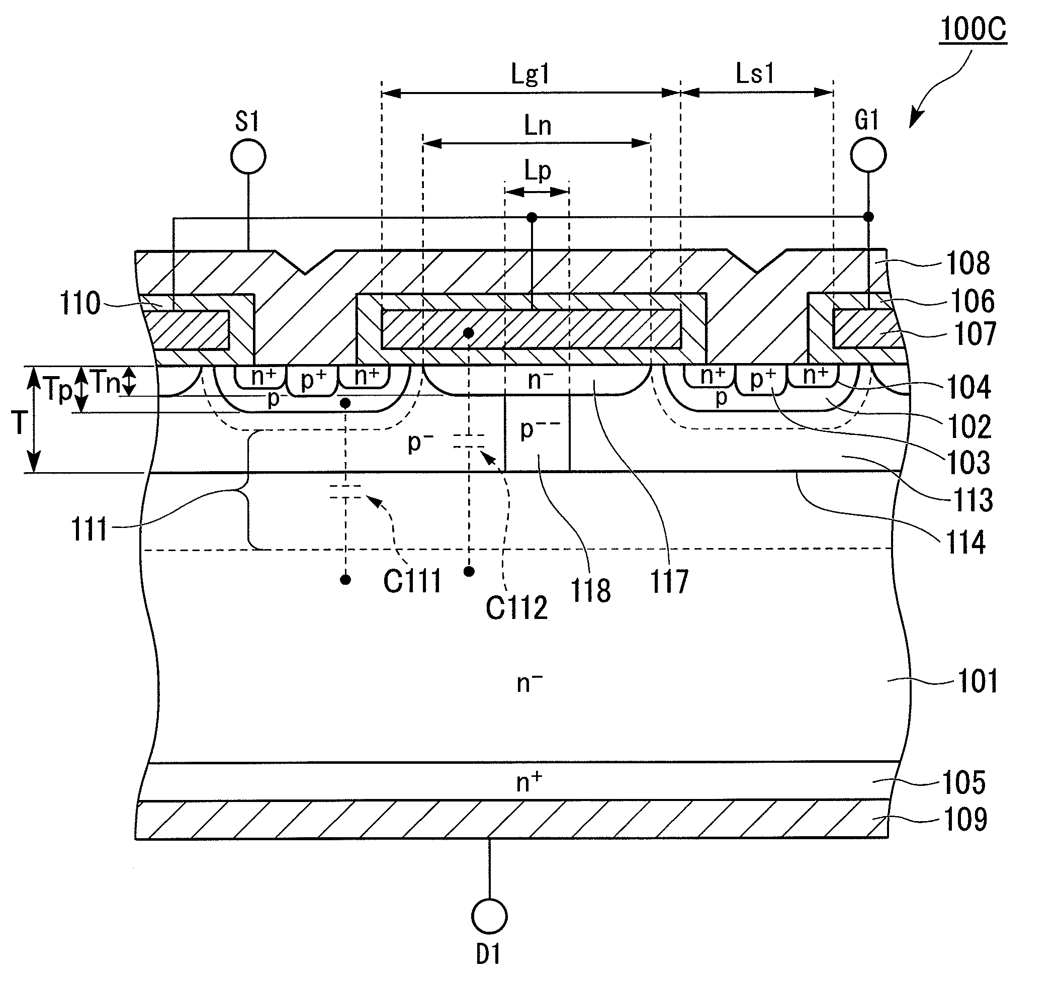
[0032]FIG. 1 is a cross-sectional view showing a schematic configuration of a semiconductor device according to a first embodiment of the invention. As shown in FIG. 1, a semiconductor device 1 of this embodiment includes a gate electrode (electrode) 12 and a source electrode 13, which are provided on a top face side of a substrate (e.g. n-type silicon) whereon an n− drift layer (first region) 11 and the like are formed, and a drain electrode 14 which is provided on a bottom face side of the n− drift layer 11. The semiconductor device 1 has a source terminal S, a gate terminal G, and a drain terminal D.

[0033]In FIG. 1, a layer designated by symbol ‘n’ has electrons as its majority carrier (first conductive layer). A layer designated by symbol ‘p’ has holes as its majority carrier (second conductive layer). Symbol ‘+’ appended to the symbols ‘n’ and ‘p’ indicates that the layer has comparatively high impurity-density, while symbol ‘−’ indicates that the layer has comparatively low im...

second embodiment

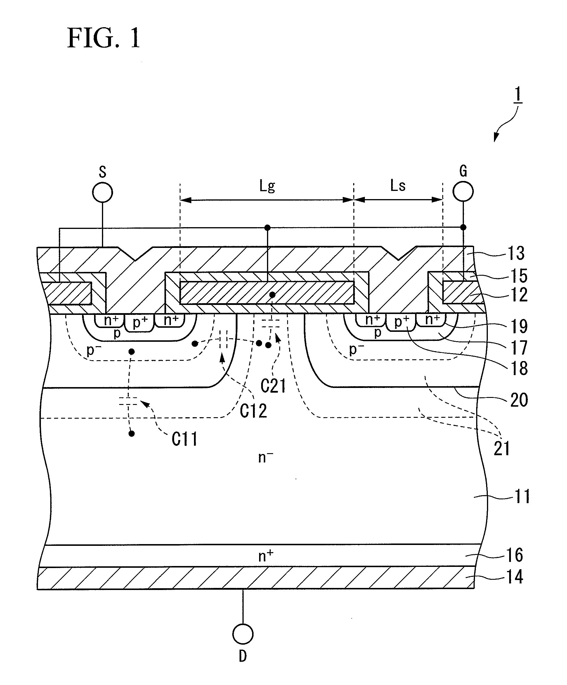
[0038]FIG. 2 is a cross-sectional view showing a schematic configuration of a semiconductor device according to a second embodiment of the invention. As shown in FIG. 2, while the configuration is roughly similar to that of the semiconductor device 1 in FIG. 1, one difference is the inclusion of a gate electrode 32 having a structure that differs from that of the gate electrode 12. The semiconductor device 1 shown in FIG. 1 includes the gate electrode 12 whose length is the length from the n+ layer 19 formed on one of adjacent p base layers 17 to the n+ layer 19 formed on the other p base layer 17. In contrast, the semiconductor device 2 of the embodiment shown in FIG. 2 includes a gate electrode 32 with an opening above a portion where the n− drift layer 11 is exposed at the surface (intermediary portion between adjacent p base layers 17).

[0039]Inclusion of the gate electrode 32 having the structure shown in FIG. 2 reduces the plan-view overlap between the n− drift layer 11 and the...

third embodiment

[0041]FIG. 3 is a cross-sectional view showing a schematic configuration of a semiconductor device according to a third embodiment of the invention. As shown in FIG. 3, a semiconductor device 3 according to this embodiment differs in that, instead of the gate electrode 12 and the oxide film 15 shown in FIG. 1, it includes a gate electrode 42 and an oxide film 45 which have different structures thereto. The semiconductor device 3 of this embodiment includes an oxide film 45 made by local oxidation of silicon (LOCOS), and a gate electrode 42 that is formed on the oxide film 45.

[0042]As shown in FIG. 3, the oxide film 45 is formed so as to be embedded in the substrate where the n-drift layer 11 and the like are formed between p base layers 17. The oxide film 45 electrically isolates the p base layers 17 from each other. For example, SiO2 can be used as the oxide film 45. Since the oxide film 45 is formed by embedding, as shown in FIG. 3, it is thick. The gate electrode 42 is formed fro...


PUM


Abstract

A semiconductor device according to the present invention includes: a first region having a first conductive type; a plurality of second regions having a second conductive type that differs from the first conductive type, and formed to be arranged in the first region; a plurality of third regions having the first conductive type and formed in the second regions; an electrode forming a channel between the first region and the third region; and a plurality of extended second regions having the second conductive type, arranged in the first region such as to individually include one of the second regions and having an impurity density that is lower than an impunity density of the second regions.

Description

BACKGROUND OF THE INVENTION[0001]1. Field of the Invention[0002]The present invention relates to a semiconductor device that can be applied in a metal oxide semiconductor field effect transistor (MOSFET) having a vertical structure, an insulated gate bipolar transistor (IGBT), a diode, and the like.[0003]Priority is claimed on Japanese Patent Application No. 2008-005992, filed Jan. 15, 2008, Japanese Patent Application No. 2008-208896, filed Aug. 14, 2008, and Japanese Patent Application No. 2008-249557, filed Sep. 29, 2008, the contents of which are incorporated herein by reference.[0004]The invention of the present application relates to inventions disclosed in Japanese Patent Application No. 2007-170732, and Japanese Patent Application No. 2008-103732, which are filed by the applicant of the present application.[0005]2. Description of Related Art[0006]Conventional power MOSFETs and solid state relays (SSR) are constituted with a semiconductor device known as a vertical double-dif...

Claims


Application Information

Patent Timeline
Patent Type & Authority Applications(United States)
IPC IPC(8): H01L29/78H01L27/00
CPCH01L29/1045H01L29/1095H01L29/42368H01L29/7802H01L29/42376H01L29/66712H01L29/7395H01L29/42372
Inventor KOMACHI, TOMONORI
Owner YOKOGAWA ELECTRIC CORP
Why Eureka
Try Eureka