Semiconductor On-Chip Repair Scheme for Negative Bias Temperature Instability

a technology of negative bias and temperature instability, applied in the field of on-chip repair of semiconductor devices, can solve the problems of negative bias temperature instability (nbti), device performance degradation away from optimal performance level, and more specifically, p-type field effect transistors (pfets),

Inactive Publication Date: 2009-07-16
GLOBALFOUNDRIES INC
View PDF9 Cites 15 Cited by
  • Summary
  • Abstract
  • Description
  • Claims
  • Application Information

AI Technical Summary

Benefits of technology

[0005]In view of the foregoing, disclosed herein are embodiments of a semiconductor chip structure and a method that incorporate a localized, on-chip, repair scheme for devices that exhibit performance degradation as a result of negative bias temperature instability (NBTI). The repair scheme utilizes a heating element above each device. The heating element is configured so that it can receive transmission line pulses and, thereby generate enough heat t

Problems solved by technology

Negative bias temperature instability (NBTI) is a phenomenon in which powered-up sub-micron complementary metal oxide semiconductor (CMOS) devices and, more specifically, p-type field effect transistors (PFETs), exhibit performance degradation over time and/or under certain use conditions.
Due

Method used


Image

  • Semiconductor On-Chip Repair Scheme for Negative Bias Temperature Instability
  • Semiconductor On-Chip Repair Scheme for Negative Bias Temperature Instability
  • Semiconductor On-Chip Repair Scheme for Negative Bias Temperature Instability

Examples


Embodiment Construction

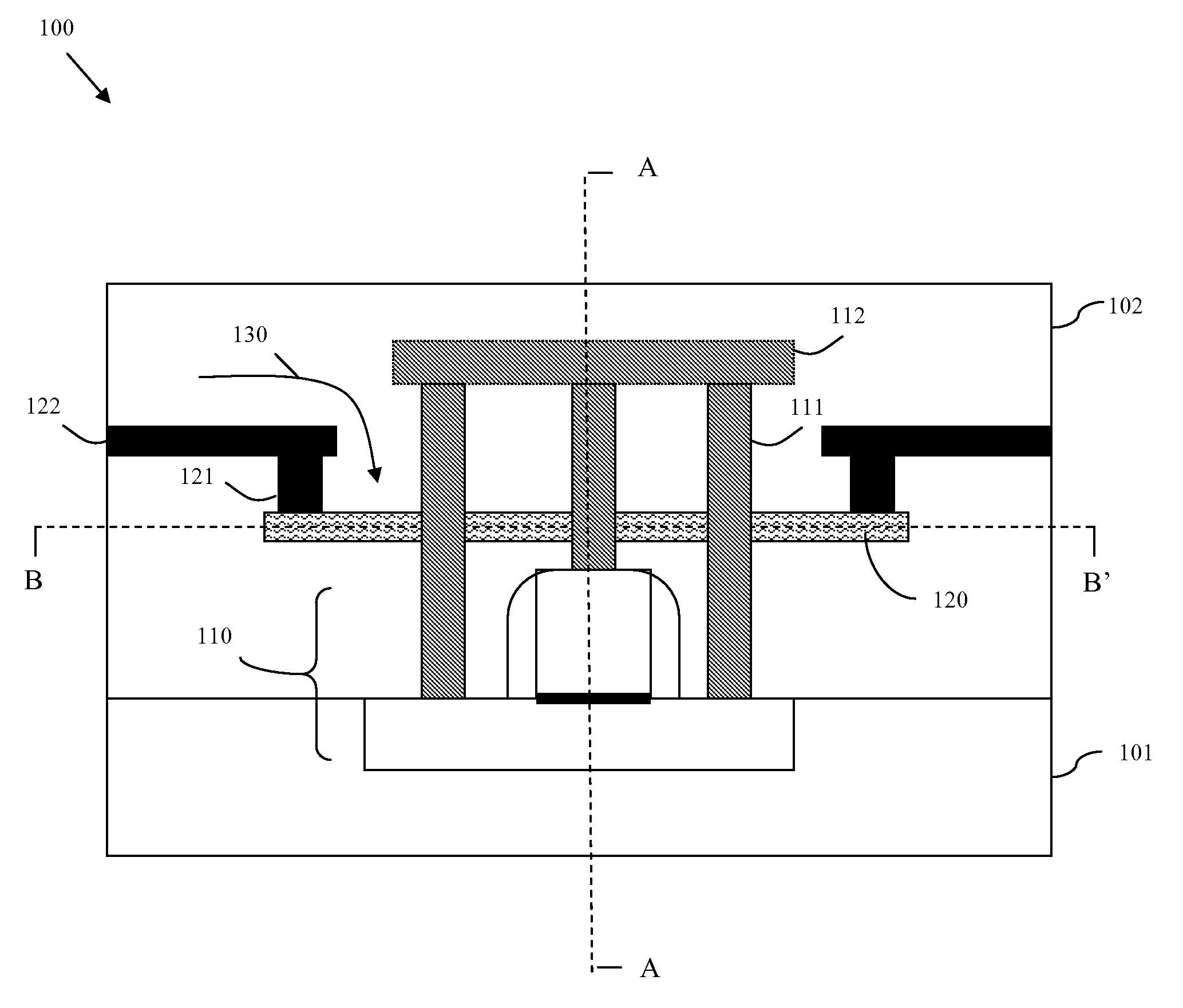
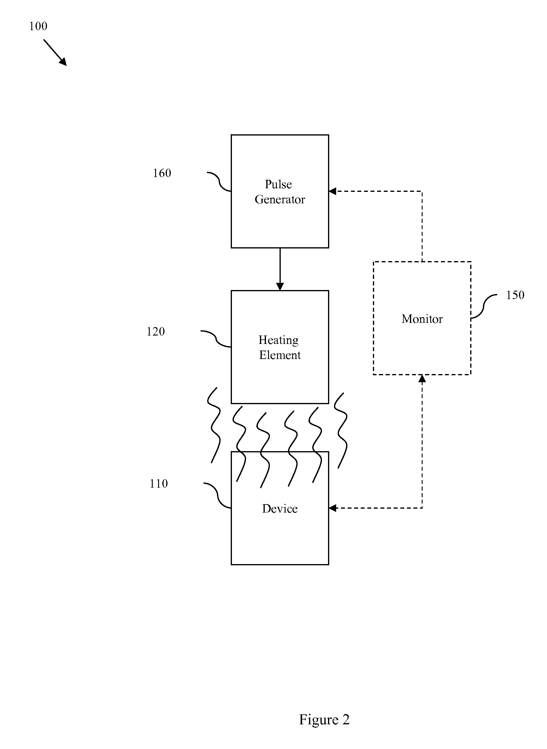
[0020]The embodiments of the invention and the various features and advantageous details thereof are explained more fully with reference to the non-limiting embodiments that are illustrated in the accompanying drawings and detailed in the following description. It should be noted that the features illustrated in the drawings are not necessarily drawn to scale. Descriptions of well-known components and processing techniques are omitted so as to not unnecessarily obscure the embodiments of the invention. The examples used herein are intended merely to facilitate an understanding of ways in which the embodiments of the invention may be practiced and to further enable those of skill in the art to practice the embodiments of the invention. Accordingly, the examples should not be construed as limiting the scope of the embodiments of the invention.

[0021]Negative bias temperature instability (NBTI) is a phenomenon in which powered-up sub-micron complementary metal oxide semiconductor (CMOS)...


PUM


Abstract

Disclosed are embodiments of a semiconductor chip structure and a method that incorporate a localized, on-chip, repair scheme for devices that exhibit performance degradation as a result of negative bias temperature instability (NBTI). The repair scheme utilizes a heating element above each device. The heating element is configured so that it can receive transmission line pulses and, thereby generate enough heat to raise the adjacent device to a temperature sufficient to allow for performance recovery. Specifically, high temperatures (e.g., between approximately 300-400° C. or greater) in the absence of bias can accelerate the recovery process to a matter of seconds as opposed to days or months. The heating element can be activated, for example, on demand, according to a pre-set service schedule, and/or in response to feedback from a device performance monitor.

Description

BACKGROUND[0001]1. Field of the Invention[0002]The embodiments of the invention generally relate to on-chip repair of semiconductor devices and, more particularly, to a semiconductor chip structure and a method that incorporate a localized, on-chip, repair scheme for devices that exhibit performance degradation as a result of negative bias temperature instability (NBTI).[0003]2. Description of the Related Art[0004]Negative bias temperature instability (NBTI) is a phenomenon in which powered-up sub-micron complementary metal oxide semiconductor (CMOS) devices and, more specifically, p-type field effect transistors (PFETs), exhibit performance degradation over time and / or under certain use conditions. This NBTI primarily causes an increase in the PFET threshold voltage and, thereby causes a reduction in the PFET drive current. Consequently, there is a need in the art for semiconductor chip structure and a method that allows for localized, on-chip, repair of devices suffering from NBTI...

Claims


Application Information

Patent Timeline
IPC IPC(8): H03K3/42H01L21/00
CPCH01L22/14H01L22/20H01L23/345H01L23/5228H01L2924/0002H01L2924/00
Inventor BOLAM, RONALD J.LEE, TOM C.SULLIVAN, TIMOTHY D.
Owner GLOBALFOUNDRIES INC
Why Eureka
Try Eureka