Integral heater assembly and method for carrier or host board of electronic package assembly

a heater and electronic package technology, applied in the field of surface mount technology (smt), can solve the problems of increasing the cost of modules, increasing the cost of high-value devices, and increasing the cost of products

Inactive Publication Date: 2013-04-18
INTEGRATED MICROWAVE
View PDF3 Cites 44 Cited by
  • Summary
  • Abstract
  • Description
  • Claims
  • Application Information

AI Technical Summary

Benefits of technology

[0012]Embodiments described herein provide for a heater assembly and method for zone-selective surface mount assembly and removal which allows a select portion of the host board to be reflowed without reflowing adjacent areas of the host board.
[0014]The use of a copper metal trace for the heater element has the advantage over tungsten that it is easy to process and of low cost. However, copper is of relatively low resistance. By forming the heater element from a relatively thin trace of copper in a circuitous or meandering path, which may be serpentine, zig-zag, spiral or of other meandering or circuitous shapes, the heater element has as much length as possible in the desired heating area, increasing the resistance. The heater element is connected to a low voltage, high current power supply in order to provide sufficient power, and thus sufficient heat to melt the solder layer affixing the surface mount module to a host board, allowing the surface mount module to be removed from the host board. Prior art does not consider the use of copper heating elements because traditionally, high resistance materials are used to make resistance heater structures. But the use of low voltages and higher currents allows copper to perform well as a heater element. The presence of copper as the “standard” conductive material for printed circuit boards makes its use very economical and practical.
[0018]With this method, the heater element does not have to heat the solder element from ambient temperature to the solder reflow temperature, which could take a long time if the module is large or the solder reflow temperature is high. The heater element generates enough heat to raise the temperature of the solder layer of the module sufficiently to melt the solder layer in a relatively short time, due to the pre-heating or concurrent oven heating of the assembly. The pre-heating or oven heating of the entire host-board raises the overall temperature of the assembly to a lower temperature which is close to, but below the solder reflow temperature, to reduce or eliminate the risk of damage to other components or modules on the board or loosening the solder connection of such devices so that they fall off the board. Using the oven reduces the amount of heat which must be generated by the heater element, which may be restricted by design parameters in some designs.
[0019]Where lower solder reflow temperatures or smaller, lower mass modules are involved, requiring less energy to raise to the solder reflow temperature, the oven heating step may be eliminated and the heater element may be used to heat the solder layer from ambient temperature (25 C) to the solder reflow temperature.

Problems solved by technology

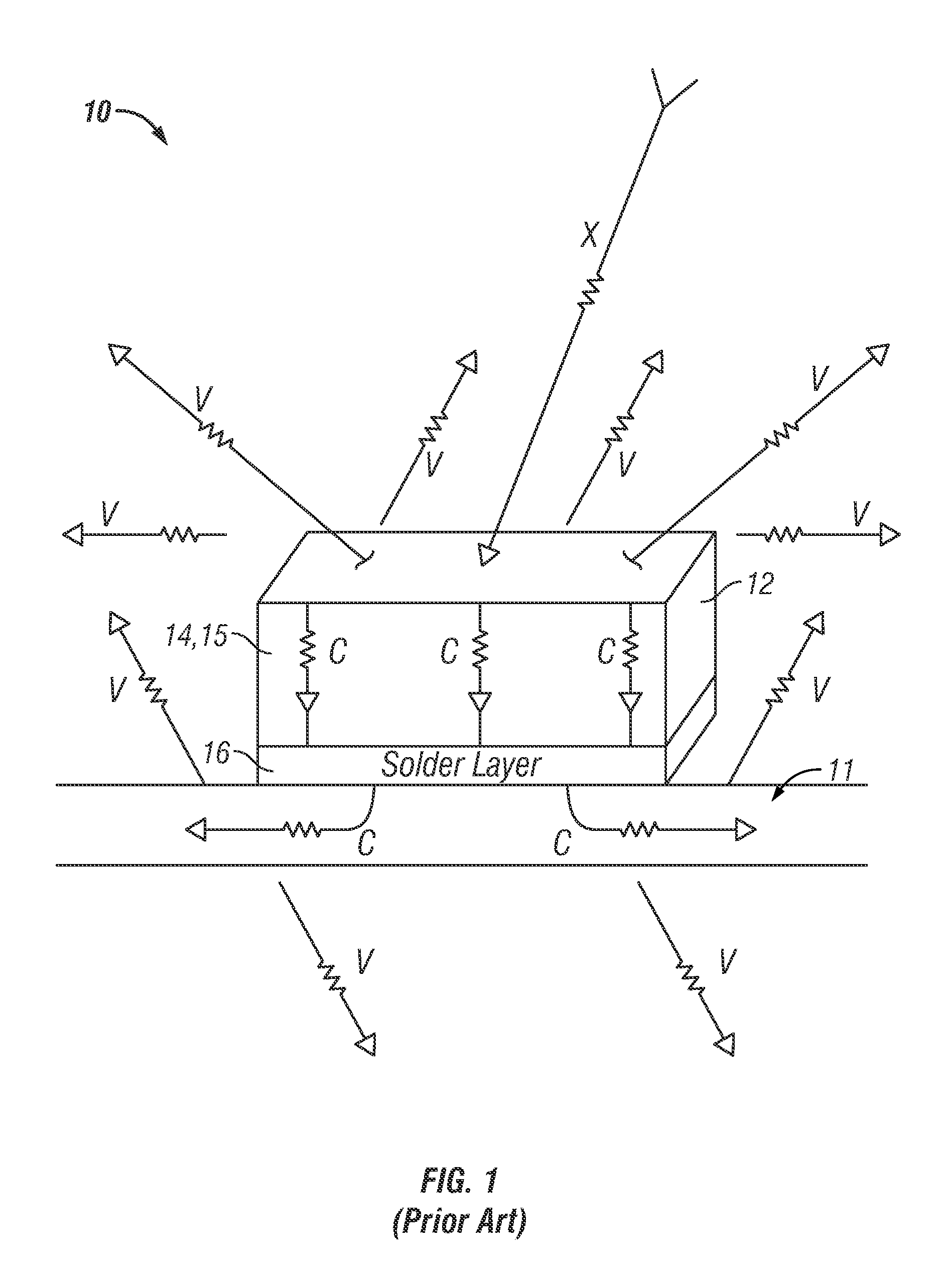
Modules are relatively expensive, high value devices, and are frequently printed circuit board or PCB based, in other words the 
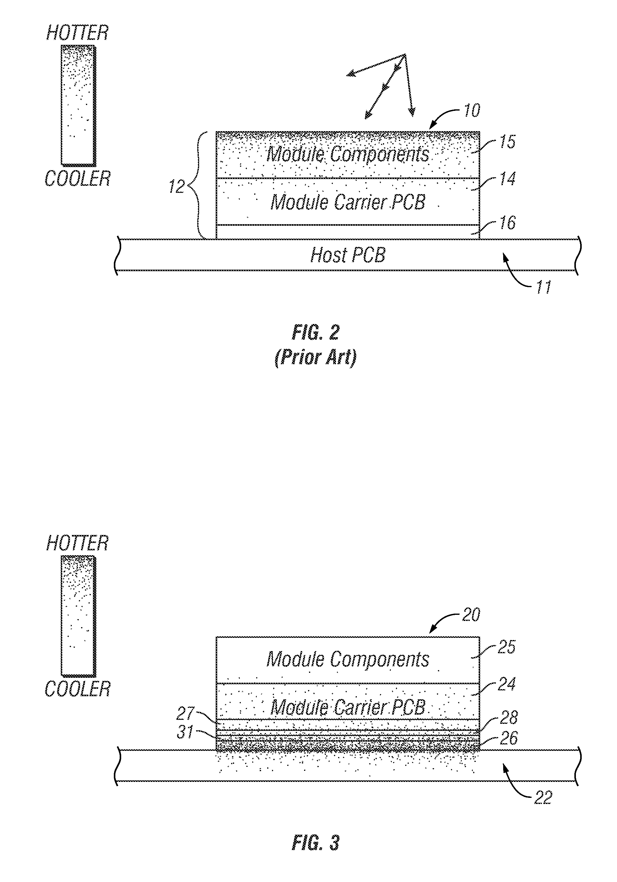
assembly is based on a carrier board, which serves as a substrate to hold the internal components and also provides a metallized mounting plane or solder interface layer, and can be thought of as a “module” which is in turn soldered to a host board which is larger than the module and may host many other components and modules.
Currently, such products are getting smaller and space constraints are increasing.
SMT modules can be particularly difficult to remove from the host board.
In order to remove an individual module from the board after installation, it is desirable to heat only a selected portion of the host board, but that is rarely possible.
Heating the entire host-board assembly past the solder reflow temperature jeopardizes the quality of the unit by wasting valuable component termination leach life, degrading solder quality.
In some cases, heating the entire board is not even possible because a secondary re-flow to facilitate replacement of a single component or module will cause other components to become damaged or to fall off.
Such systems do not work well with large modules or modules with poor thermal conductivity from top to mounting plane.
The hot air temperatures necessary to reflow the solder which is under the module usually damages the components inside.
Hot air at 215° C. cannot overcome the thermal masses and losses associated with a typical mounting configuration and still reflow solder under the module, which probably melts at 183 C or higher, and therefore the module cannot be removed without damage.
Even preheating the host board to assist in overcoming these losses, which is the most successful tactic, rarely produces the desired result and usually results in damage to one or more modules which were previously surface mounted on the board.
Reinstallation of a module is also rarely possible using current state of the art techniques.
Frequently, a manufacturer will cheat and use a soldering iron to re-install a module.
The resulting air gaps under the module degrade thermal performance, degrade RF performance, provide inferior mechanical strength, and are generally known to be undesirable.
In RF filter module installations above approximately 300 MHz, this practice is particularly detrimental and degrades return loss (VSWR) and rejection (attenuation of undesired RF energy) as a result.
There are many limitations to hot shoe technology.
This means that custom parts need custom shoes.
Reinstallation of modules or components using this technique is very difficult or impossible.
Host board damage is likely.
For large mass modules, the time needed for module removal makes host board damage inevitable.
For large area modules, the technique does not work at all because reflow cannot be achieved near the center of the module, and therefore it cannot be removed.
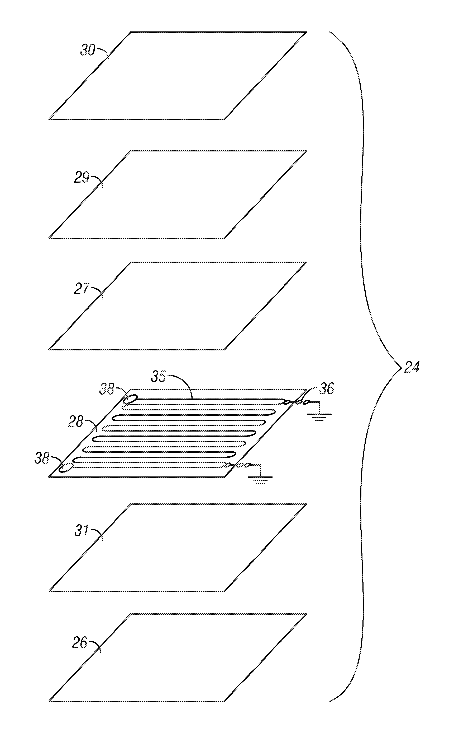
The technique described in this patent is limited to MCMs with ceramic substrates and printed wiring of tungsten or like materials having lossy characteristics akin to that of tungsten.
Tungsten is a high resistance, exotic material and is both expensive and difficult to process.
Traditional epoxy-glass circuit board materials (such as FR-4) are not available clad with tungsten, and the addition of tungsten would make production and processing virtually impossible.
The known heating methods involving multiple heater elements are not applicable to many types of electronic components including larger scale surface mount modules.
However, copper is of relatively low resistance.
Prior art does not consider the use of copper heating elements because traditionally, high resistance materials are used to make resistance heater structures.
Other suitable highly conductive metals for the heater element are gold or silver, but these are more expensive than copper.
With this method, the heater element does not have to heat the solder element from ambient temperature to the solder reflow temperature, which could take a long time if the module is large or the solder reflow temperature is high.
Using the oven reduces the amount of heat which must be generated by the heater element, which may be restricted by design parameters in some designs.

Method used


Image

  • Integral heater assembly and method for carrier or host board of electronic package assembly
  • Integral heater assembly and method for carrier or host board of electronic package assembly
  • Integral heater assembly and method for carrier or host board of electronic package assembly

Examples


Embodiment Construction

[0034]Certain embodiments as disclosed herein provide for a surface mount assembly in which a heater layer is embedded in one or more surface mount modules each having a carrier board holding internal components and a metallized mounting plane or solder interface layer. In another embodiment, a heater layer with plural heater zones is embedded in a host board on which multiple surface mount modules are mounted.

[0035]After reading this description it will become apparent to one skilled in the art how to implement the invention in various alternative embodiments and alternative applications. However, although various embodiments will be described herein, it is understood that these embodiments are presented by way of example only, and not limitation. As such, this detailed description of various alternative embodiments should not be construed to limit the scope or breadth of the present invention.

[0036]In the following description, the term “dielectric layer” means a layer of dielectr...


PUM

PropertyMeasurementUnit
thicknessaaaaaaaaaa
lengthaaaaaaaaaa
poweraaaaaaaaaa

Abstract

A multilayer printed circuit board has an embedded heater layer having at least one elongated heater element trace of copper which is densely arranged in a predetermined circuitous path over at least part of the area of the board. The heater element has inputs configured for connection to a standard high current, low voltage power supply, and may also have ground connections for selective connection to a ground layer. The heater layer may be embedded in a carrier board of a surface mount module close to the lower solder interface layer, or may be embedded in a host board of an electronics assembly close to the mounting surface.

Description

BACKGROUND[0001]1. Field of the Invention[0002]The present invention relates generally to surface mount technology (SMT) as used in manufacture of electronic products, and is particularly concerned with electronic package assemblies comprising surface mount components and / or subassemblies (SMT devices), and with integral heater assemblies and methods for heating solder layers securing SMT devices to allow removal from host boards.[0003]2. Related Art[0004]The trend in electronics packaging is to eliminate discrete or separate electronic components and make assemblies smaller by relying on very large scale integration (VLSI) integrated circuits or electronic modules. This allows designers of printed circuit assemblies and products to purchase a module for a particular desired function from a manufacturer, without having to design a circuit to perform the function and in a very compact form. In a module, several chips or other components are usually present in a miniaturized form. For...

Claims


Application Information

Patent Timeline
Patent Type & Authority Applications(United States)
IPC IPC(8): H05K7/20H05K13/00
CPCH05K1/0212H05K1/141H05K1/167Y10T29/49821H05K3/3494H05K2203/176H05K3/22Y10T29/49822H05B3/0014H05B3/06H05B3/12H05B3/16H05K1/181H05K13/0486
Inventor SLOANE, JEFFREY
Owner INTEGRATED MICROWAVE
Why Eureka
Try Eureka