

Nonvolatile memory and three-state FETs using cladded quantum dot gate structure
- Summary
- Abstract
- Description
- Claims
- Application Information
AI Technical Summary
Benefits of technology
Problems solved by technology
Method used
Image

Examples
Embodiment Construction
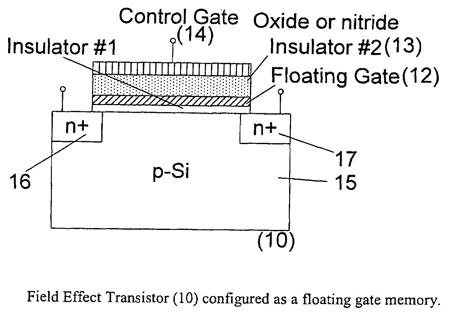
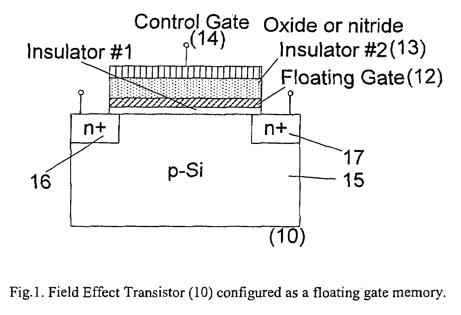
[0042]FIG. 1. Cross-sectional schematic of a conventional floating gate nonvolatile memory. Here the Si field-effect transistor (FET) has two gates. The first gate is the floating gate (12), which is deposited on a thin insulator layer (11), and holding the desired charge determining the state of the memory [0 or 1], and the second gate (14) serves as the control gate which is separated by an insulator layer (13) for the memory. The source (16): and drain (17) regions are shown as n+ regions in p-Si substrate (15). The control gate could be simple metal layer (14) or appropriately doped poly-Si layer (not shown here) with the metal contact layer.
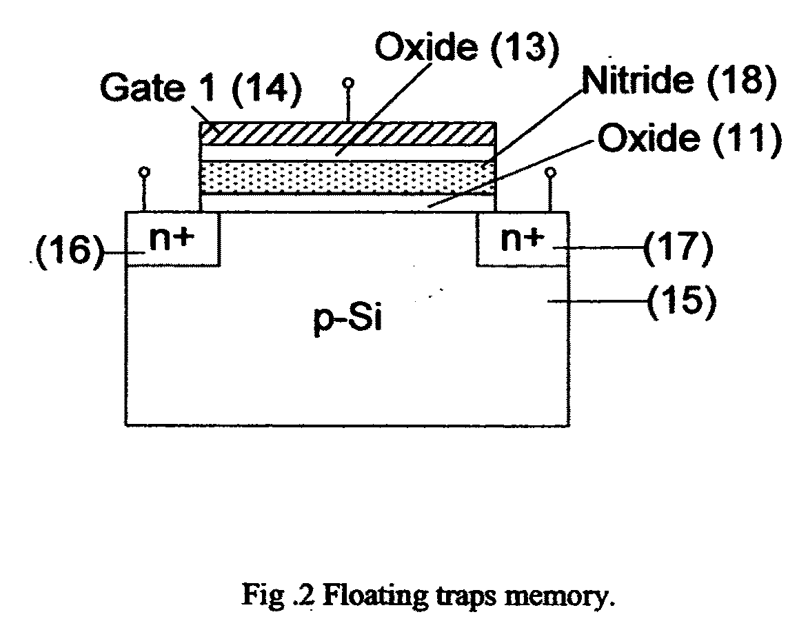
[0043]FIG. 2. Cross-sectional schematic of a conventional floating trap nonvolatile memory in SONOS [Si (15), oxide (11), nitride (18), oxide (13), poly-Si (not shown under gate metal 14 for simplicity)] configuration. Here the charge in the gate is trapped at the interface between nitride, Si3N4, (18) and gate insulator (11) SiO2. The Si3N4...
PUM
 Abstract
Description
Claims
Application Information