

Photovoltaic devices having metal oxide electron-transport layers
a photovoltaic device and electron transport technology, applied in the direction of nanoinformatics, sustainable manufacturing/processing, final product manufacturing, etc., can solve the problems of reducing device performance and efficiency not reaching the level required for commercial applications
- Summary
- Abstract
- Description
- Claims
- Application Information
AI Technical Summary
Benefits of technology
Problems solved by technology
Method used
Image

Examples
example 1
Photovoltaic Devices Having Zinc Oxide Nanoparticle and Benzoic Acid Monolayer Electron-Transporting Layers
[0106]This example describes a solution-based processing method for fabricating PV devices that include an SAM-modified ZnO / metal bilayer electron-collecting electrode. A series of conjugated carboxylic-acid SAMs with various dipoles was used to tune the contact property between the ZnO layer and three different metal electron-collecting electrodes: Al, Ag, and Au. Self-assembled molecules used in this example include para-substituted benzoic-acid (BA-X) molecules where X is: —OCH3, —CH3, —H, —SH, —CF3, or —CN. The devices have large efficiencies, even when high work-function metals, such as Ag and Au, were used as electron-collecting electrodes.
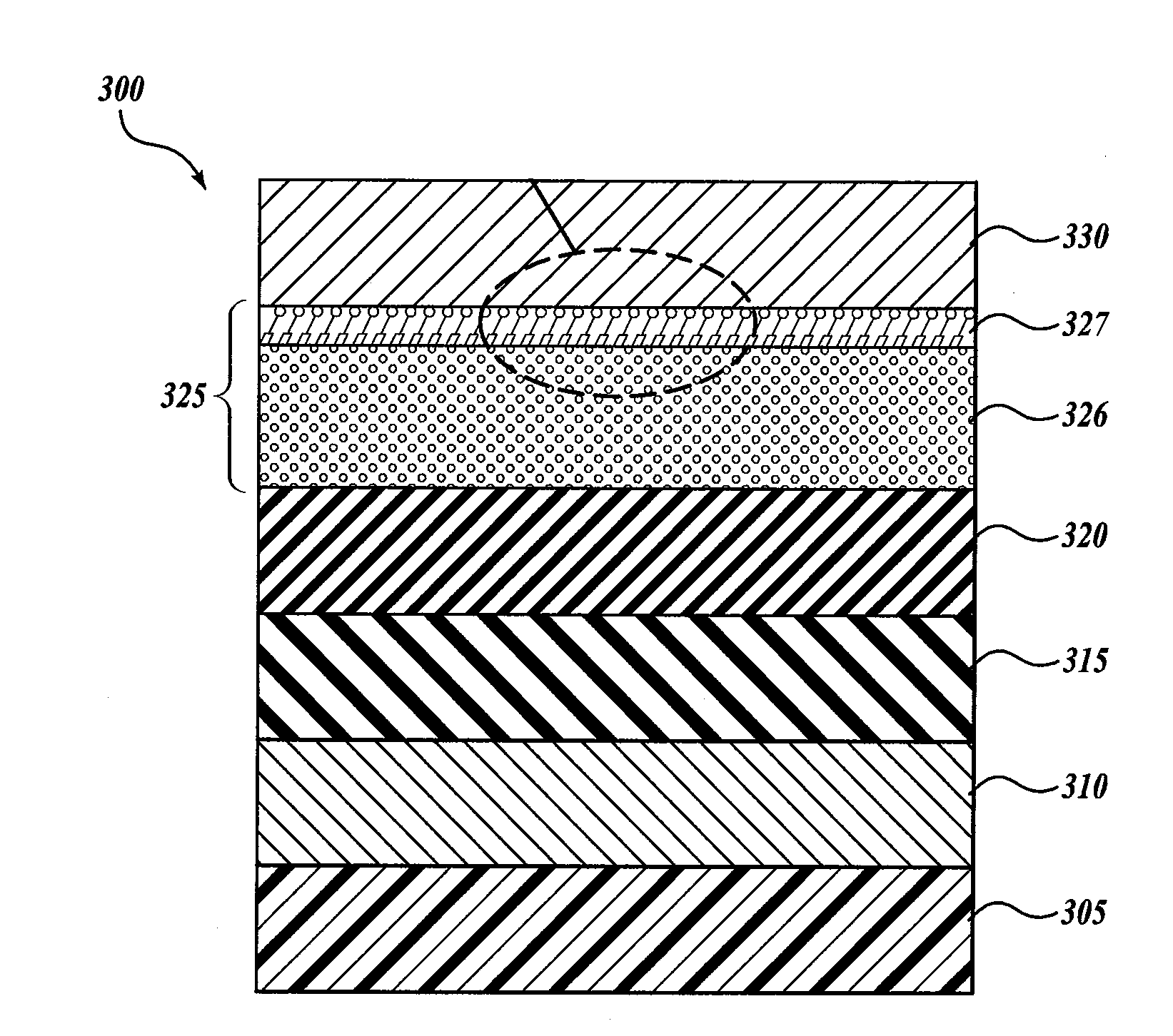
[0107]The structure of the PV devices used in this Example are illustrated in FIG. 3A. Device fabrication began with ITO-coated glass substrates (15Ω / □) cleaned in an ultrasonic bath with detergent, DI water, acetone, and isopropyl alco...
example 2
Photovoltaic Devices Having Zinc Oxide Nanoparticles Modified with Aliphatic Chain SAMs
[0120]This example describes a solution-based processing method for fabricating PV devices that include an SAM-modified ZnO / metal bilayer cathode. Similar to Example 1, a series of conjugated carboxylic-acid SAMs with various dipoles were used to tune the contact property between the ZnO layer and three different metal electron-collecting electrodes: Al, Ag, and Au. Self-assembled molecules used in this example include lauric acid (LA), mercaptoundecanoic acid (MUA), and perfluorotetradecanoic acid (PFTDA). The devices show dramatically improved efficiencies, even when high work-function metals, such as Ag and Au, were used as electron-collecting electrodes.
[0121]Device fabrication: ITO-coated glass substrates (15 Ω / □) were cleaned in an ultrasonic bath with detergent, DI water, acetone, and isopropyl alcohol and then dried under a N2 stream. The substrates were then treated with oxygen plasma for...
example 3
Inverted Photovoltaic Devices Having Fullerene-Containing Self-Assembled Monolayers Modifying Metal Oxide Electron-Transport Layers
[0127]In this example, a spin-coating process is employed to modify the metal oxide (ZnO) interface of inverted PV devices with a fullerene-SAM. The SAM reduces the device series resistance by passivating the inorganic surface trap states as well as enhances the electronic coupling at ZnO / photovoltaic-layer interface. The SAM helps mediate forward charge transfer to reduce back recombination at the interface leading to improved fill factors and photocurrent densities. In addition, some inverted devices were fabricated in an ambient environment and performed comparably to those fabricated in an inert environment.
[0128]The PV devices used in this example are “inverted” because the transparent electrode, ITO, is used as the electron-collecting electrode (cathode), whereas traditional devices use ITO as the hole-collecting electrode (anode).
[0129]To fabricat...
PUM
| Property | Measurement | Unit |
|---|---|---|
| electron mobility | aaaaa | aaaaa |
| temperature | aaaaa | aaaaa |
| concentration | aaaaa | aaaaa |
Abstract
Description
Claims
Application Information