Magnetoresistive element and method of manufacturing the same

a technology of magnetoresistive elements and manufacturing methods, applied in nanoinformatics, instruments, record information storage, etc., can solve the problems of insufficient conventional spin filter layer, weak field signal of recording medium, and difficult to distinguish conventional read head

Active Publication Date: 2009-07-30
KK TOSHIBA
View PDF27 Cites 56 Cited by
  • Summary
  • Abstract
  • Description
  • Claims
  • Application Information

AI Technical Summary

Benefits of technology

[0021]repeating two or more modules each comprising depositing a metal layer and ...

Problems solved by technology

As a result, a magnetic field signal from the recording medium becomes very weak to make a conventional read head difficult to distinguish between “0” and “1”.
However, it came to be fou...

Method used


Image

  • Magnetoresistive element and method of manufacturing the same
  • Magnetoresistive element and method of manufacturing the same
  • Magnetoresistive element and method of manufacturing the same

Examples


example 1

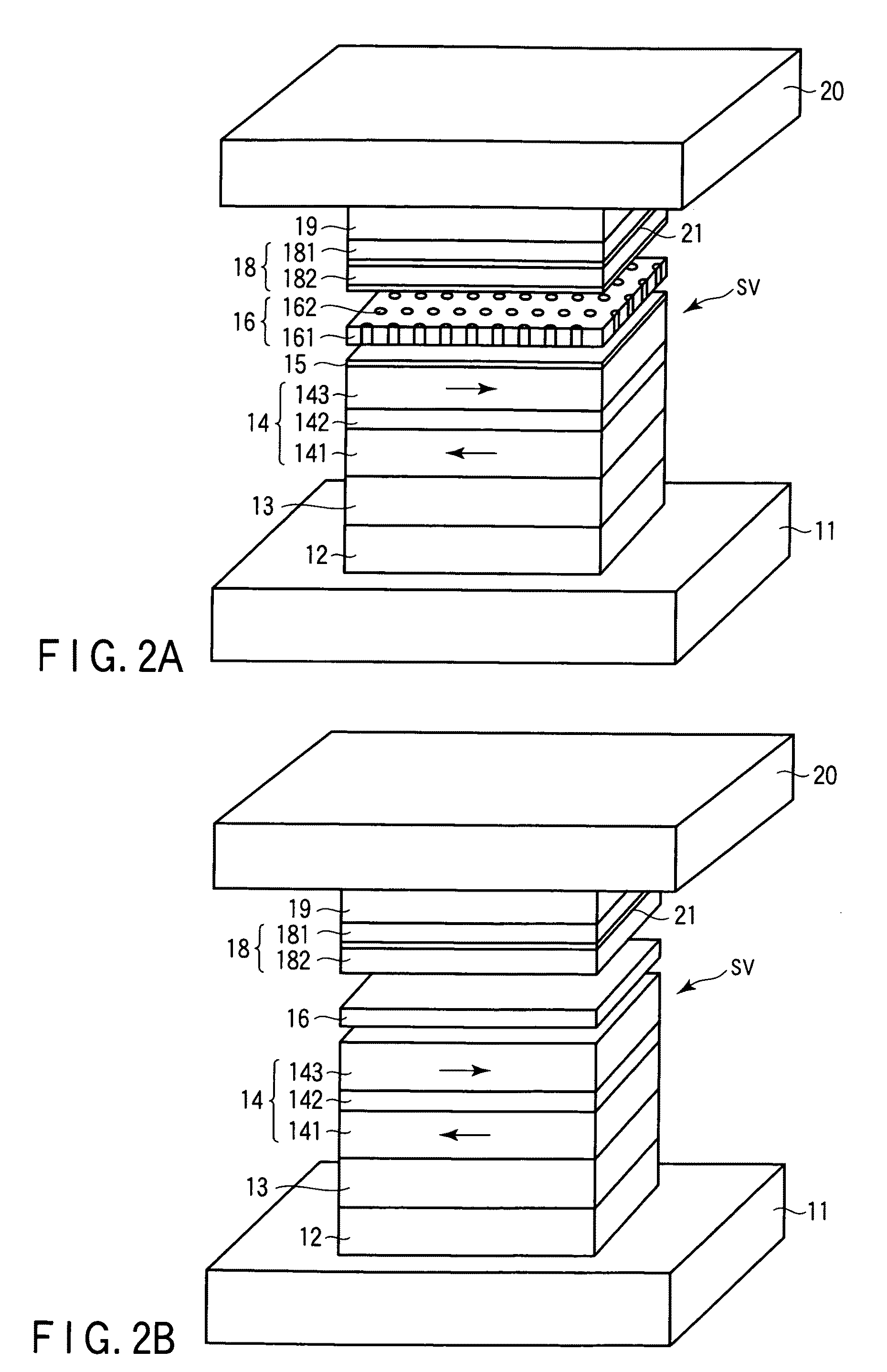
[0161]The magnetoresistive element shown in FIG. 2B was prepared in this examples. The magnetoresistive element in Example 1 is structured as follows: Lower electrode 11[0162]Underlayer 12: Ta [1 nm] / Ru [2 nm][0163]Pinning layer 13: Ir22Mn78 [7 nm][0164]Pinned layer 14: Co90Fe10 [4 nm] / Ru [0.85 nm] / Co90Fe10 [4 nm][0165]Spacer layer (all metal) 16: Cu [3 nm][0166]Lower free layer 181: Co90Fe10 [2 nm][0167]SF layer 21: (Nitride of Fe80Co20 [0.4 nm])×5 layers prepared by the method in FIGS. 5A to 5E[0168]Upper free layer 182: Co90Fe10 [2 nm][0169]Cap layer 19[0170]Upper electrode 20.

[0171]Now, a method of forming the free layer including the SF layer after the layers to the spacer layer 16 are deposited will be described. To produce a usual spin-valve film, layers are stacked to the space layer 16, and then the free layer is deposited in one step. When the free layer including the SF layer such as in this example is formed, a magnetic layer having half the thickness of the usual free l...

example 2

[0207]The magnetoresistive element shown in FIG. 3B was manufactured by using the following materials:[0208]Lower electrode 11[0209]Underlayer 12: Ta [1 nm] / Ru [2 nm][0210]Pinning layer 13: Ir22Mn78 [7 nm][0211]Lower pinned layer 141: Co90Fe10 [4 nm][0212]Antiferromagnetic coupling layer 142: Ru [0.85 nm][0213]First upper pinned layer 144: Co90Fe10 [2 nm][0214]SF layer 21: (Nitride of Fe80Co20 [0.4 nm])×5 layers prepared by the method in FIGS. 5A to 5E[0215]Second upper pinned layer 145: Co90Fe10 [2 nm][0216]Spacer layer (all metal) 16: Cu [3 nm][0217]Free layer 18: Co90Fe10 [4 nm][0218]Cap layer 19: Cu [1 nm] / Ru [10 nm][0219]Upper electrode 20.

example 3

[0220]The magnetoresistive element shown in FIG. 3A was manufactured by using the following materials:[0221]Lower electrode 11[0222]Underlayer 12: Ta [1 nm] / Ru [2 nm][0223]Pinning layer 13: Ir22Mn78 [7 nm][0224]Lower pinned layer 141: Co90Fe10 [4 nm][0225]Antiferromagnetic coupling layer 142: Ru [0.85 nm][0226]First upper pinned layer 144: Co90Fe10 [2 nm][0227]SF layer 21: (Nitride of Fe80Co20 [0.4 nm])×5 layers prepared by the method in FIGS. 5A to 5E[0228]Second upper pinned layer 145: Co90Fe10 [2 nm][0229]Spacer layer (CCP-NOL) 16: Al2O3 insulating layer 161 and Cu current paths 162[0230]Free layer 18: Co90Fe10 [4 nm][0231]Cap layer 19: Cu [1 nm] / Ru [10 nm][0232]Upper electrode 20.


PUM


Abstract

A magnetoresistive element includes a magnetoresistive film including a magnetization pinned layer, a magnetization free layer, an intermediate layer arranged between the magnetization pinned layer and the magnetization free layer, a cap layer arranged on the magnetization pinned layer or on the magnetization free layer, and a functional layer formed of an oxygen- or nitrogen-containing material and arranged in the magnetization pinned layer, or in the magnetization free layer, and a pair of electrodes which pass a current perpendicularly to a plane of the magnetoresistive film, in which a crystalline orientation plane of the functional layer is different from a crystalline orientation plane of its upper or lower adjacent layer.

Description

CROSS-REFERENCE TO RELATED APPLICATIONS[0001]This application is based upon and claims the benefit of priority from prior Japanese Patent Application No. 2008-019365, filed Jan. 30, 2008, the entire contents of which are incorporated herein by reference.BACKGROUND OF THE INVENTION[0002]1. Field of the Invention[0003]The present invention relates to a magnetoresistive element which detects magnetism by passing a sense current in a direction perpendicular to the plane of a magnetoresistive film, and a method of manufacturing the same.[0004]2. Description of the Related Art[0005]At present, magnetic recording apparatuses such as HDD (hard disk drive) are used in applications of personal computers, portable audio / video players, video cameras and car navigation system. A further increase in recording capacity of HDD is desired with the expansion of applications. For increasing recording capacity without increasing the volume of HDD, further improvement in recording density per unit area ...

Claims


Application Information

Patent Timeline
IPC IPC(8): G11B5/127G11B5/48B05D3/00
CPCB82Y10/00B82Y25/00G01R33/093G11B5/3906H01L43/12G11C11/16H01L27/228H01L43/08H01L43/10G11B2005/3996G11C11/161H10B61/22H10N50/10H10N50/01H10N50/85G11B5/127G11B5/39
Inventor MURAKAMI, SHUICHIFUKUZAWA, HIDEAKIYUASA, HIROMIFUJI, YOSHIHIKO
Owner KK TOSHIBA
Why Eureka
Try Eureka