Process with saturation at low etch amount for high contact bottom cleaning efficiency for chemical dry clean process

a technology of chemical dry cleaning and contact bottom surface, which is applied in the direction of semiconductor devices, electrical equipment, semiconductor/solid-state device details, etc., can solve the problems of damage to the underlying surface, significantly lower oxide removal at and very low cleaning efficiency of the contact hole bottom surfa

Inactive Publication Date: 2009-07-30
APPLIED MATERIALS INC
View PDF6 Cites 23 Cited by
  • Summary
  • Abstract
  • Description
  • Claims
  • Application Information

AI Technical Summary

Benefits of technology

[0012]In yet another embodiment, a method of forming a metal contact comprises depositing a metal on a substrate in a first vacuum environment, annealing the substrate at conditions sufficient to provide a metal silicide layer, depositing an insulating cover layer on the metal silicide layer, forming a contact hole in the insulating cover layer exposing a portion of the metal silicide layer, transferring the substrate from the first vacuum environment to a second vacuum environment, wherein the exposed portion of the metal silicide layer at least partially oxidizes during the transfer, and exposing the exposed portion of the at least partially oxidized silicide layer to a reactive species in the second vacuum environment to remove the at least partially oxidized silicide layer while substantially maintaining the shape of the contact hole.

Problems solved by technology

Sputter etch processes have been used in an attempt to clean contact hole bottom surfaces; however, such techniques may damage the underlying surface.
However, during this process, the upper and sidewall surfaces of the contact opening are exposed to the oxide cleaning chemicals for a longer period of time than the bottom contact oxide surface.
This results in significantly lower oxide removal at the contact hole bottom surface than at the upper and sidewall surfaces; hence, the contact hole bottom surface cleaning efficiency is very low.
Accordingly, the contact resistance may be elevated, resulting in inefficiency of the device, and / or the geometry of the contact opening may be compromised, resulting in current leakage.

Method used


Image

  • Process with saturation at low etch amount for high contact bottom cleaning efficiency for chemical dry clean process
  • Process with saturation at low etch amount for high contact bottom cleaning efficiency for chemical dry clean process
  • Process with saturation at low etch amount for high contact bottom cleaning efficiency for chemical dry clean process

Examples


Embodiment Construction

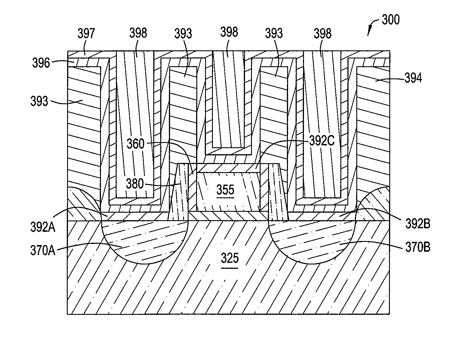
[0017]As will be explained in greater detail below, a substrate having a contact surface at least partially disposed thereon is treated to remove metal oxides or other contaminants prior to contact level metallization. The term “contact surface” as used herein refers to a layer of material that includes a metal silicide that can form part of a gate electrode. In one or more embodiments, the metal silicide can be nickel silicide, cobalt silicide, titanium silicide or any combinations thereof. The metal silicide can also include tungsten, Ti / Co alloy silicide, Ti / Ni alloy silicide, Co / Ni alloy silicide and Ni / Pt silicide.

[0018]The term “substrate” as used herein refers to a layer of material that serves as a basis for subsequent processing operations and includes a “contact surface.” For example, the substrate can include one or more conductive metals, such as aluminum, copper, tungsten, or combinations thereof. The substrate can also include one or more nonconductive materials, such ...


PUM


Abstract

A method for removing oxides from the bottom surface of a contact hole is provided. The method provides efficient cleaning of the bottom surface without distortion of the contact hole upper and sidewall surfaces.

Description

BACKGROUND OF THE INVENTION[0001]1. Field of the Invention[0002]Embodiments of the present invention generally relate to methods for forming electronic devices. More particularly, embodiments of the present invention generally relate to methods for cleaning contact hole bottom surfaces in the formation of electronic devices.[0003]2. Description of the Related Art[0004]In the fabrication of an active electronic device, such as a Metal Oxide Silicon Field Effect Transistor (“MOSFET”), the electrodes and interconnecting pathways include silicide layers formed by depositing a refractory metal on bare silicon and annealing the layer to produce the metal silicide layer. A dielectric layer is then deposited over the metal silicide, and a contact hole is formed through the dielectric layer to the surface of the metal silicide. The contact hole is then filled with a bulk metal to complete the contact.[0005]In a typical fabrication process, the metal silicide may be formed on a substrate in o...

Claims


Application Information

Patent Timeline
Patent Type & Authority Applications(United States)
IPC IPC(8): H01L21/4763H01L21/302
CPCH01L21/02063H01L21/28518H01L29/78H01L29/665H01L21/76814H01L23/485
Inventor LU, XINLIANGYANG, HAICHUNGE, ZHENBINKAO, CHIEN-TEHCHANG, MEI
Owner APPLIED MATERIALS INC
Why Eureka
Try Eureka