Method of forming fine pattern using block copolymer

a technology of copolymer and fine pattern, which is applied in the field of fine pattern manufacturing of semiconductor devices, can solve the problems of difficult application and limit to improving resolution

Inactive Publication Date: 2009-07-30
SAMSUNG ELECTRONICS CO LTD
View PDF12 Cites 41 Cited by
  • Summary
  • Abstract
  • Description
  • Claims
  • Application Information

AI Technical Summary

Benefits of technology

[0008]The present technology provides a method of forming a fine pattern of a semiconductor device, which can readily realize a pattern having a fine pitch which is required in manufacturing a highly integrated semiconductor device that overcomes a resolution limit in a photolithography process.

Problems solved by technology

When only a photolithography technology using a top-down method is used in order to form a fine pattern for manufacturing a semiconductor device, there may be a limit to improving the resolution due to the wavelength of a light source and the resolution limit of an optical system.
However, a conventional method of forming a fine pattern using self-assembly of molecules is still in an experimental stage, and thus is difficult to apply when trying to realize a fine pattern for actually manufacturing a semiconductor device.

Method used


Image

  • Method of forming fine pattern using block copolymer
  • Method of forming fine pattern using block copolymer
  • Method of forming fine pattern using block copolymer

Examples


Embodiment Construction

[0024]The present technology will now be described more fully with reference to the accompanying drawings, in which exemplary embodiments of the technology are shown.

[0025]The technology may, however, be embodied in many different forms and should not be construed as being limited to the embodiments set forth herein; rather, these embodiments are provided so that this disclosure will be thorough and complete, and will fully convey the concept of the technology to those of ordinary skill in the art. Elements and regions in the drawings are briefly illustrated. Thus, the present technology shall not be limited by relative sizes or intervals illustrated in the drawings.

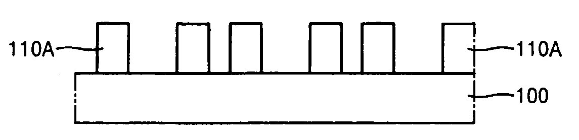
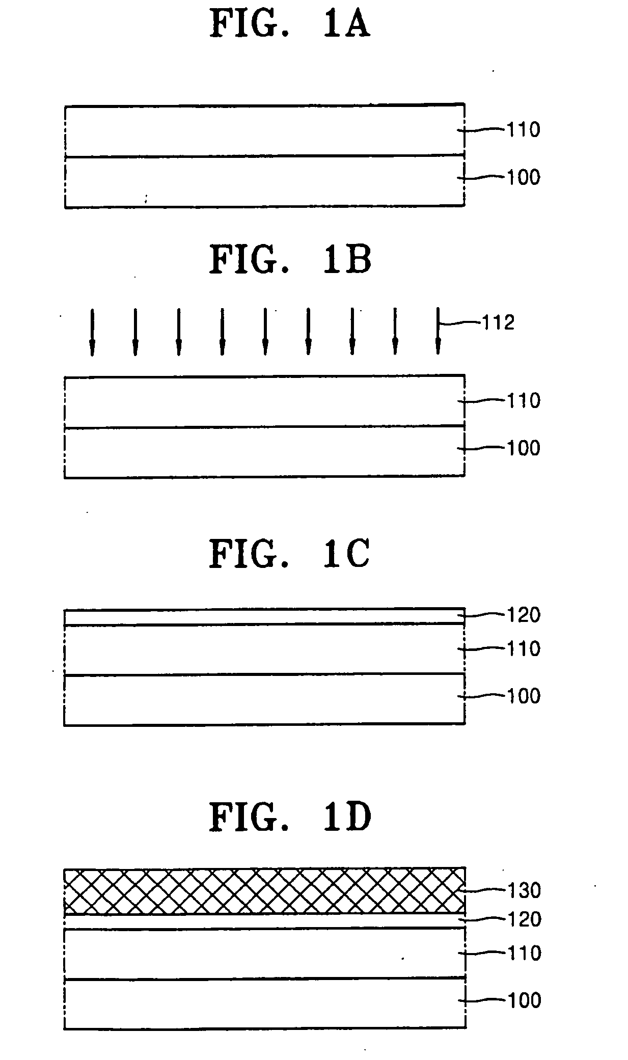
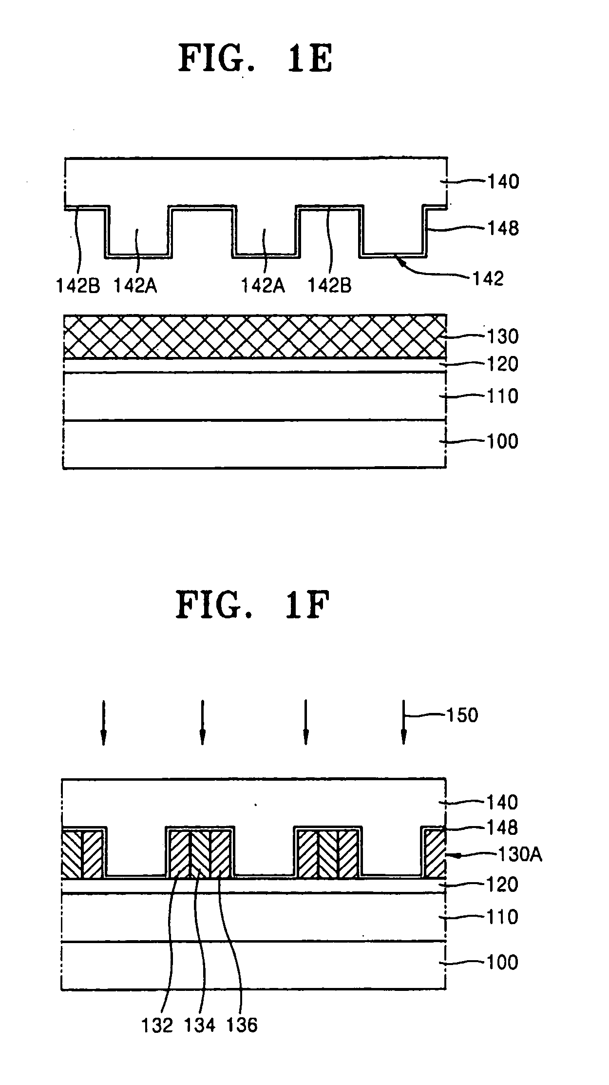
[0026]FIGS. 1A through 1K are diagrams for describing a method of forming a fine pattern 110A according to an embodiment of the present technology;

[0027]Referring to FIG. 1A, an etching layer 110 is formed on a substrate 100.

[0028]The substrate 100 may be a semiconductor substrate, such as silicon.

[0029]The etching layer...


PUM

PropertyMeasurementUnit
thicknessaaaaaaaaaa
thicknessaaaaaaaaaa
thicknessaaaaaaaaaa

Abstract

Provided is a method of forming a fine pattern using a block copolymer. The method comprises forming a coating layer including a block copolymer having a plurality of repeating units on a substrate. A mold is provided having a first pattern comprising a plurality of ridges and valleys. The first pattern is transferred from the mold into the coating layer. Then, a self-assembly structure is formed comprising a plurality of polymer blocks aligned in a direction guided by the ridges and valleys of the mold thereby rearranging the repeating units of the block copolymer within the coating layer by phase separation while the coating layer is located within the valleys of the mold. A portion of the polymer blocks are removed from among the plurality of polymer blocks and a self-assembly fine pattern of remaining polymer blocks is formed.

Description

CROSS-REFERENCE TO RELATED PATENT APPLICATION[0001]This application claims the benefit of Korean Patent Application No. 10-2008-0009059, filed on Jan. 29, 2008, in the Korean Intellectual Property Office, the disclosure of which is incorporated herein in its entirety by reference.BACKGROUND[0002]1. Field of the Technology[0003]The present technology relates to a method of forming a fine pattern for manufacturing a semiconductor device, and more particularly, to a method of forming a fine pattern using a block copolymer.[0004]2. Description of the Related Art[0005]As the integration of semiconductor devices has increased, a plane area occupied by each unit cell has decreased. In response to such a decrease in the plane area, a design rule of a nano-scale critical dimension (CD) that is smaller than several to several tens of nanometers is applied. Accordingly, a new technology for forming a fine pattern, such as a fine contact hole pattern having a nano-scale opening size or a fine l...

Claims


Application Information

Patent Timeline
Patent Type & Authority Applications(United States)
IPC IPC(8): H01L21/311
CPCB81C1/00031B81C2201/0149B81C2201/0198B82Y10/00B82Y30/00H01L21/32139G03F7/0002H01L21/0337H01L21/3086H01L21/31144H01L21/312B82Y40/00H01L21/02118H01L21/02107H01L21/0274
Inventor YOON, DONG-KIKIM, HYUN-WOOYI, SHI-YONGNA, HAI-SUBKIM, KYOUNG-TAEKJANG, YUN-KYEONG
Owner SAMSUNG ELECTRONICS CO LTD
Why Eureka
Try Eureka