Electron emission device and display device using the same

Active Publication Date: 2009-08-06
TSINGHUA UNIV +1
View PDF12 Cites 5 Cited by
  • Summary
  • Abstract
  • Description
  • Claims
  • Application Information

AI Technical Summary

Problems solved by technology

Diode type FEDs can be used for character display, but are unsatisfactory for applications requiring high-resolution display images, because of they are relatively non-uniform and there is difficulty in controlling their electron emission.
Areas of the gate holes in the metal grid are often more than 100 μm2, so the electron emission device cannot satisfy some needs requiring great accuracy.
The uniform

Method used


Image

  • Electron emission device and display device using the same
  • Electron emission device and display device using the same
  • Electron emission device and display device using the same

Examples


Embodiment Construction

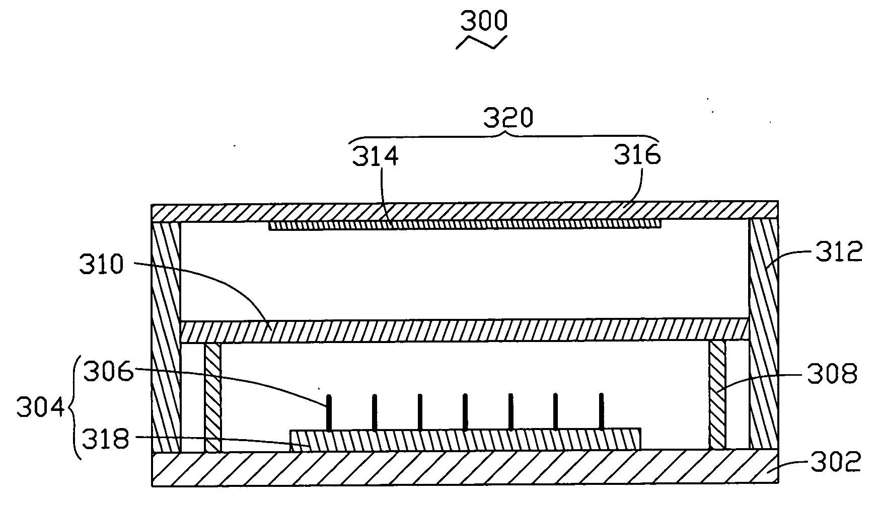
[0016]References will now be made to the drawings to describe the exemplary embodiments of the electron emission device and display device using the same, in detail.

[0017]Referring to FIG. 1, an electron emission device 10 includes a substrate 12, a cathode electrode 14, and an insulting supporter 20. The cathode electrode 14 and the insulting supporter 20 are disposed on the substrate 12. Further included is a gate electrode 22 formed on a top surface of the insulting supporter 20. The gate electrode 22 is electrically insulted from the cathode electrode 14 by the insulating supporter 20.

[0018]The substrate 12 includes a sheet of insulative plate composed of an insulating material, such as glass, silicon, ceramic, etc. The substrate 12 is used to support the cathode electrode 14. The shape of the substrate 12 can be determined according to practical needs. In the present embodiment, the substrate 12 is a ceramic substrate.

[0019]The cathode electrode 14 can be a field emission catho...


PUM


Abstract

An electron emission device includes a cathode device and a gate electrode. The gate electrode is separated and insulted from the cathode device. The gate electrode includes a carbon nanotube layer having a plurality of spaces. A display device includes a cathode device, an anode device spaced from the cathode electrode and a gate electrode. The gate electrode is disposed between the cathode device and the anode device. The cathode device, the anode device and the gate electrode are separated and insulted from each other. The gate electrode comprises a carbon nanotube layer having a plurality of spaces.

Description

RELATED APPLICATIONS[0001]This application is related to applications entitled, “ELECTRON EMISSION DEVICE AND DISPLAYING DEVICE USING THE SAME”, filed ______ (Atty. Docket No. US18589); “ELECTRON EMISSION DEVICE AND DISPLAYING DEVICE USING THE SAME”, filed ______ (Atty. Docket No. US18590). The disclosure of the respective above-identified application is incorporated herein by reference.BACKGROUND[0002]1. Technical Field[0003]The invention relates to an electron emission device and a display device using the electron emission device.[0004]2. Discussion of Related Art[0005]Electron emission displays are new, rapidly developing in flat panel display technologies. Compared to conventional technologies, e.g., cathode-ray tube (CRT) and liquid crystal display (LCD) technologies, Field Electron emission Displays (FEDs) are superior in having a wider viewing angle, low energy consumption, a smaller size, and a higher quality display.[0006]Generally, FEDs can be roughly classified into diod...

Claims


Application Information

Patent Timeline
IPC IPC(8): H01J1/90
CPCH01J3/021H01J3/027H01J2329/463H01J31/127H01J2203/0232H01J29/467
Inventor XIAO, LINLIU, LIANGJIANG, KAI-LIFAN, SHOU-SHAN
Owner TSINGHUA UNIV
Why Eureka
Try Eureka