Light emitting device and electronic apparatus

a technology of light emitting devices and electronic devices, which is applied in the direction of discharge tubes/lamp details, discharge tubes luminescnet screens, electric discharge lamps, etc., can solve the problems of difficult to manufacture image display apparatuses, increased manufacturing difficulty, and difficult to allow liquid droplets or ink droplets to be widely penetrated into corner parts

Active Publication Date: 2009-08-06
SEIKO EPSON CORP
View PDF6 Cites 73 Cited by
  • Summary
  • Abstract
  • Description
  • Claims
  • Application Information

AI Technical Summary

Benefits of technology

[0046]Since the above-described electronic apparatus includes the above-described various light emitting devices, the electronic apparatus can be manufactured in an easy manner and can display a high-definition image.

Problems solved by technology

However, in order to satisfy this requirement, there is a problem that it is difficult to manufacture the image display apparatus.
In such a case, the difficulty in manufacture is increased further.
However, there is also a problem in the technology disclosed in JP-A-2001-185354.
In other words, the liquid droplets or the ink droplets have a predetermined surface tension, and thus, for example, in a case where the shape of the opening part is angled, it is difficult to allow the liquid droplets or the ink droplets to be widely penetrated into corner parts.

Method used


Image

  • Light emitting device and electronic apparatus
  • Light emitting device and electronic apparatus
  • Light emitting device and electronic apparatus

Examples


modified example 1

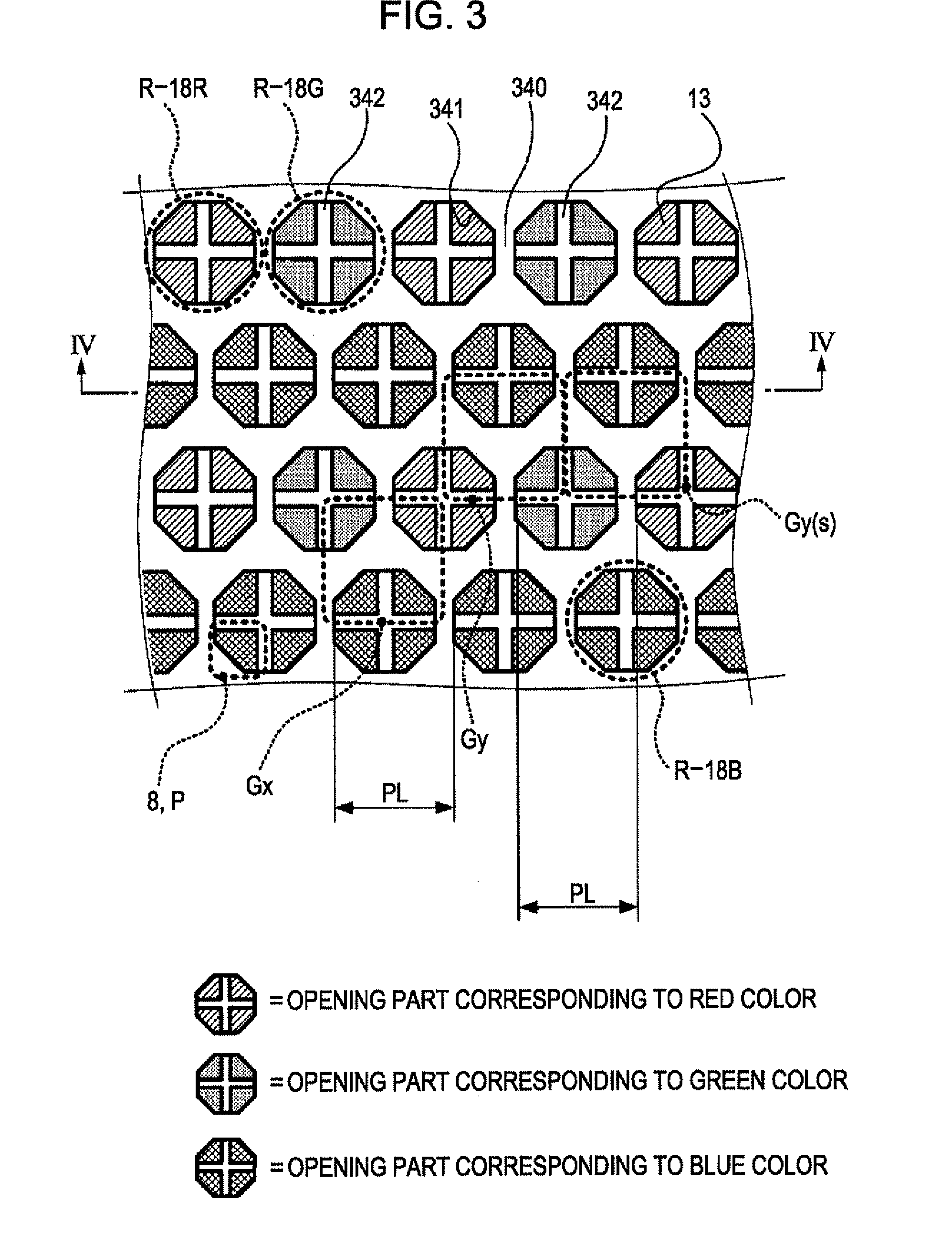
[0141]For example, as shown in FIG. 9, the red opening parts R-18R, the green opening parts R-18G, and the blue opening parts R-18B may be arranged so as to form a precise rectangular state. In such a case, the pixel Gx1 corresponding to the pixel Gx shown in FIG. 3 is configured as shown in FIG. 9 (the pixel corresponding to the “pixel Gy” is not shown in the figure. This applies to each drawing (excluding FIG. 13) according to modified examples 2 to 6).

modified example 2

[0142]Alternatively, the red opening parts R-18R, the green opening parts R-18G, and the blue opening parts R-18B may be arranged as shown in FIG. 10. In FIG. 10, the red opening parts R-18R and the green opening parts R-18G are arranged in every other row and are alternately arranged along the direction of the row, which is not different from the configuration of FIG. 3. In addition, the blue opening parts R-18B are aligned in rows adjacent to the rows in which the red opening parts R-18R and the green opening parts R-18G are aligned, which is the same as that of FIG. 3.

[0143]However, in FIG. 10, the blue opening parts R-18B are arranged in every other position along the direction of the row. In other words, since the blue opening parts R-18B are aligned to have an arrangement pitch of PL1, the red opening parts R-18R and the green opening parts R-18G are aligned to have an arrangement pitch of PL2 (here, PL2=(½)·PL1). Accordingly, in the form shown in FIG. 10, between the blue ope...

modified example 3

[0149]For example, the “opening part” and the “pixel electrode” according to an embodiment of the invention may have shapes as shown in FIG. 11. In FIG. 11, the red opening part R1-18R, the green opening part R1-18G, and the blue opening part R1-18B have an approximate quadrilateral shape. However, each corner of the quadrilateral shape is formed to be round. On the other hand, the pixel electrode 131 has an approximately precise circular shape.

[0150]In addition, the shape of the electrode separating layer 343 in the plan view is as shown in FIG. 11 in accordance with the relationship between the shapes of the opening parts R1-18R, R1-18G, and R1-18B and the shape of four pixel electrodes 131 that are aligned for each opening part. In addition, in FIG. 11, a pixel Gx3 corresponding to the pixel Gx shown in FIG. 3 is configured as shown in FIG. 11.


PUM


Abstract

A light emitting device includes a substrate, a plurality of light emitting elements that is formed on the substrate, and a partition wall layer that is formed on the substrate so as to form a plurality of opening parts in the plan view. Each of the plurality of light emitting elements includes a pixel electrode, an opposing electrode, and a light emitting function layer interposed between the pixel electrode and the opposing electrode. One of the light emitting function layers is formed to be assigned to each of the plurality of opening parts, and a plurality of the pixel electrodes is formed to be fitted into each of the plurality of opening parts. One pixel of the light emitting device includes the light emitting element that includes at least one of the pixel electrodes fitted into one of the plurality of opening parts, and at least one of the pixel electrodes that is fitted into the one of the plurality of opening parts that is adjacent to each other.

Description

BACKGROUND[0001]1. Technical Field[0002]The present invention relates to a light emitting device that emits light by using electroluminescence and an electronic apparatus.[0003]2. Related Art[0004]As a light emission source that is a thin type and is light-weighted, an OLED (organic light emitting diode), that is, an organic EL (electro luminescent) element is provided. The organic EL element has a structure in which an organic thin film of at least one layer formed of an organic material is interposed between a pixel electrode and an opposing electrode. When a current flows between both the electrodes, a current simultaneously flows through the organic thin film, and thereby, the organic thin film or the organic EL element emits light.[0005]When a plurality of the organic EL elements is aligned and emission or non-emission of each of the organic EL elements is appropriately controlled, an image or the like having desired meaning and content can be displayed.[0006]As the above-descr...

Claims


Application Information

Patent Timeline
Patent Type & Authority Applications(United States)
IPC IPC(8): H01J1/62
CPCH01L27/3246H01L51/5203H01L51/0003H10K59/122H10K71/12H10K59/805H10K50/805
Inventor KITABAYASHI, ATSUSHI
Owner SEIKO EPSON CORP
Why Eureka
Try Eureka