Density multiplication and improved lithography by directed block copolymer assembly

a technology of density multiplication and lithography, which is applied in the field of density multiplication and improved lithography by directed block copolymer assembly, can solve the problem of feature placement error and the difference in feature placement of patterns, and achieve the effect of increasing density and quality, and increasing the total number of pattern features in the block copolymer film

Active Publication Date: 2009-08-06
WISCONSIN ALUMNI RES FOUND +1
View PDF39 Cites 106 Cited by
  • Summary
  • Abstract
  • Description
  • Claims
  • Application Information

AI Technical Summary

Benefits of technology

[0003]Methods to pattern substrates with dense periodic nanostructures that combine top-down patterning tools and self-assembling block copolymer materials are provided. According to various embodiments, the methods involve chemically patterning a substrate, depositing a block copolymer film on the chemically patterned substrate, and allowing the block copolymer to self-assemble in the presence of the chemically patterned substrate, thereby producing a pattern in the block copolymer film that is improved over the substrate pattern in terms pattern feature size, shape, and uniformity, as well as regular spacing between arrays of features and between the features within each array as compared to the substrate pattern. In certain embodiments, the density and total number of pattern features in the block copolymer film is also increased as compared to the substrate pattern. High density and quality nanoimprint templates and other nanopatterned structures are also provided.

Problems solved by technology

According to certain embodiments, the feature placement error is the difference in feature placement of the pattern from the ideal periodic placement.

Method used


Image

  • Density multiplication and improved lithography by directed block copolymer assembly
  • Density multiplication and improved lithography by directed block copolymer assembly
  • Density multiplication and improved lithography by directed block copolymer assembly

Examples


Embodiment Construction

1. Introduction

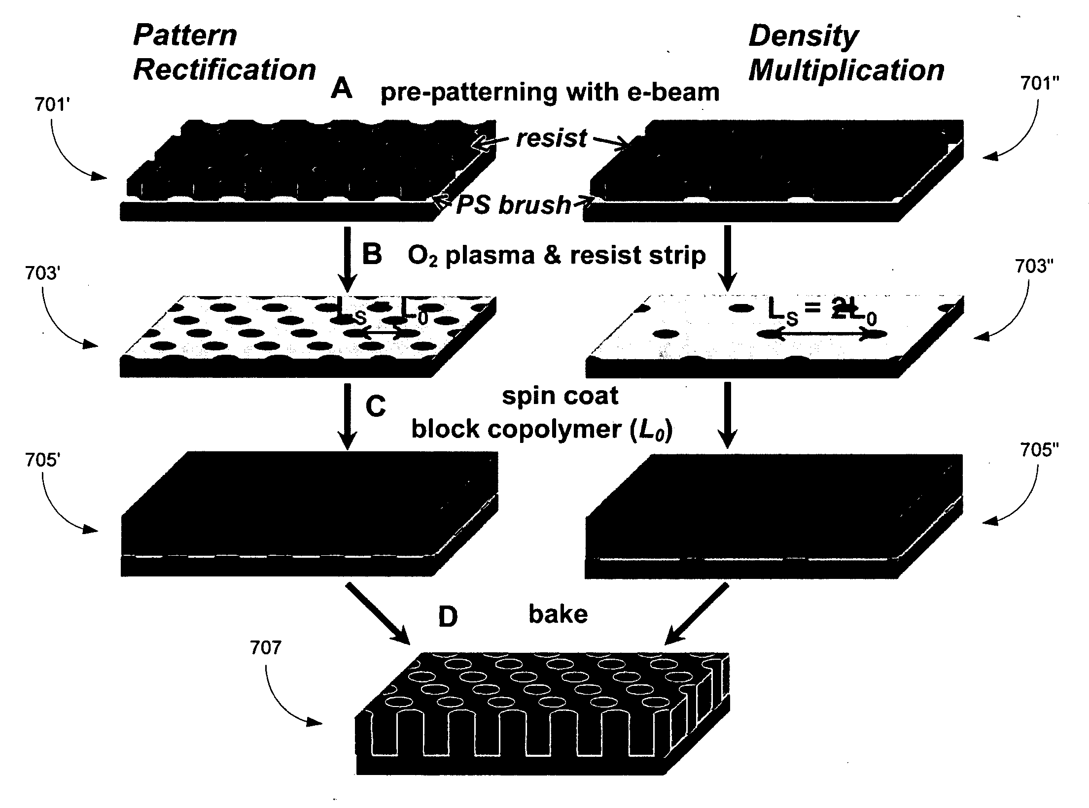
[0040]Reference will now be made in detail to specific embodiments of the invention. Examples of the specific embodiments are illustrated in the accompanying drawings. While the invention will be described in conjunction with these specific embodiments, it will be understood that it is not intended to limit the invention to such specific embodiments. On the contrary, it is intended to cover alternatives, modifications, and equivalents as may be included within the spirit and scope of the invention. In the following description, numerous specific details are set forth in order to provide a thorough understanding of the present invention. The present invention may be practiced without some or all of these specific details. In other instances, well known process operations have not been described in detail in order not to unnecessarily obscure the present invention.

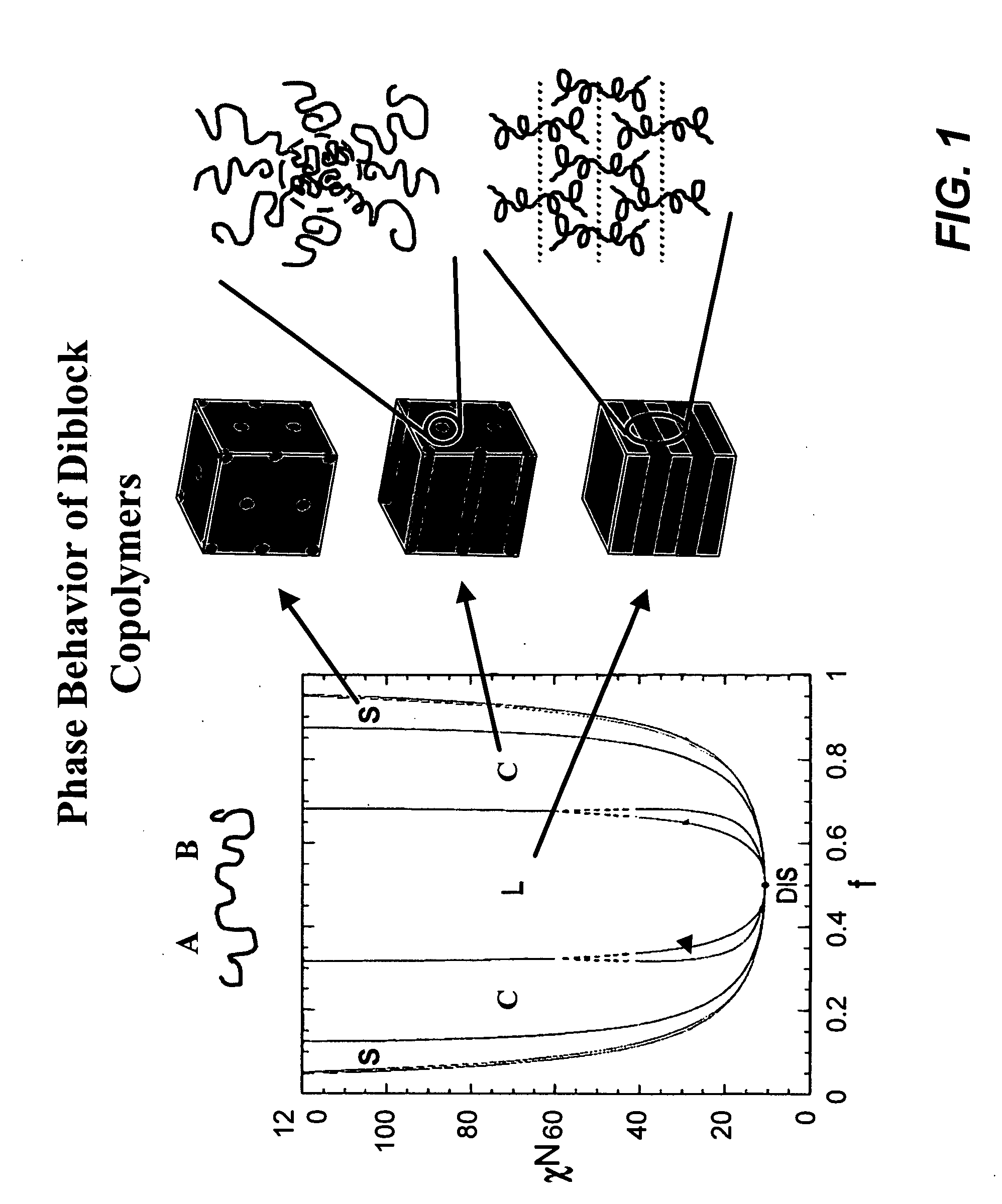
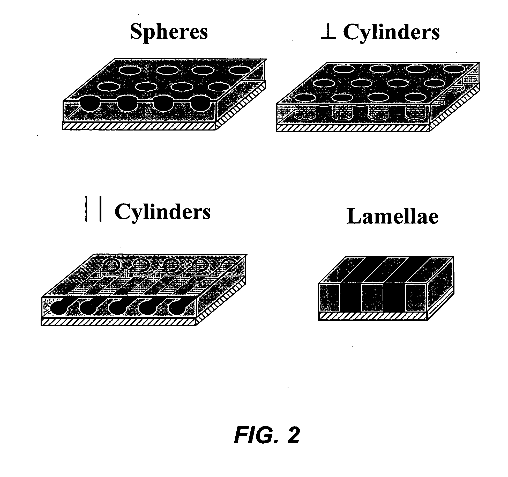
[0041]Self-assembling materials spontaneously form structures at length scales of interest in nanotechnolog...


PUM


Abstract

Methods to pattern substrates with dense periodic nanostructures that combine top-down lithographic tools and self-assembling block copolymer materials are provided. According to various embodiments, the methods involve chemically patterning a substrate, depositing a block copolymer film on the chemically patterned imaging layer, and allowing the block copolymer to self-assemble in the presence of the chemically patterned substrate, thereby producing a pattern in the block copolymer film that is improved over the substrate pattern in terms feature size, shape, and uniformity, as well as regular spacing between arrays of features and between the features within each array compared to the substrate pattern. In certain embodiments, the density and total number of pattern features in the block copolymer film is also increased. High density and quality nanoimprint templates and other nanopatterned structures are also provided.

Description

CROSS-REFERENCE TO RELATED APPLICATIONS[0001]This application claims benefit under 35 U.S.C. 119(e) of the following U.S. Provisional Applications: U.S. Provisional Application No. 61 / 005,721, filed Dec. 7, 2007; U.S. Provisional Application No. 61 / 068,912, filed Mar. 10, 2008; and U.S. Provisional Application No. 61 / 189,085, filed Aug. 15, 2008. All of these applications are incorporated by reference herein in their entireties and for all purposes.BACKGROUND OF THE INVENTION[0002]As the development of nanoscale mechanical, electrical, chemical and biological devices and systems increases, new processes are needed to fabricate nanoscale devices and components. This is especially true as the scale of these structures decreases to the tens of nanometers and below. The creation and replication of patterns is a key operation in the fabrication process. For example, in chip fabrication, optical lithography tools may be used to print the circuit patterns. However, optical lithography is p...

Claims


Application Information

Patent Timeline
Patent Type & Authority Applications(United States)
IPC IPC(8): G06K9/00
CPCB81C1/00031B81C2201/0149B82Y10/00B82Y30/00G11B5/855G03F7/0002G11B5/743G11B5/746G11B5/82B82Y40/00B05D5/00G11B5/84
Inventor NEALEY, PAUL FRANKLINKANG, HUIMANDETCHEVERRY, FRANCOISDE PABLO, JUAN J.RUIZ, RICARDOALBRECHT, THOMAS
Owner WISCONSIN ALUMNI RES FOUND
Why Eureka
Try Eureka