Semiconductor electronic device

a technology of electronic devices and semiconductors, applied in the direction of semiconductor/solid-state device manufacturing, semiconductor devices, electrical devices, etc., can solve the problems of large differences in lattice constant and thermal expansion coefficient between si and gan, cracks in gan layers, and increase in strain included, so as to reduce warp and large breakdown voltage

Active Publication Date: 2009-08-13
FURUKAWA ELECTRIC CO LTD
View PDF6 Cites 38 Cited by
  • Summary
  • Abstract
  • Description
  • Claims
  • Application Information

AI Technical Summary

Benefits of technology

[0012]It is an object of the present invention to provide a semicond...

Problems solved by technology

However, there are large differences in lattice constant and thermal expansion coefficient between Si and GaN.
Therefore, when a GaN layer is grown directly on a Si substrate, a large tensile strain is created in the GaN layer, which is a cause of a concave warp of the epitaxial wafer and/or a degradation of a crystal quality.
Further, when the immanent strain is too large, cra...

Method used


Image

  • Semiconductor electronic device
  • Semiconductor electronic device
  • Semiconductor electronic device

Examples


first embodiment

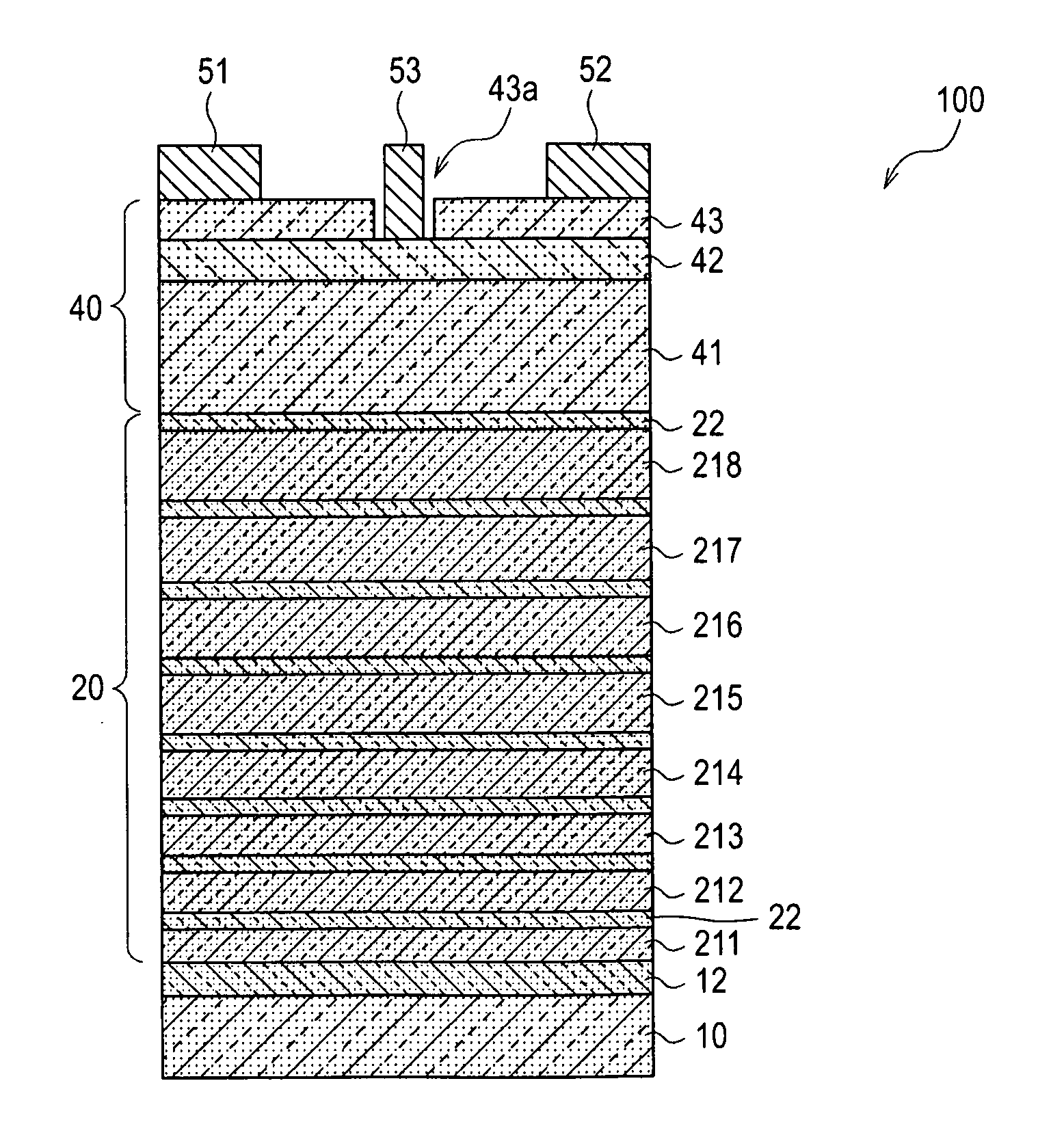
[0054]FIG. 1 is a cross sectional view schematically showing a field effect transistor according to a first embodiment of the present invention. The field effect transistor 100 is a high electron mobility transistor (HEMT), and includes a substrate 10 of single crystal Si having a (111) face as a principal face, a buffer layer 20 formed on the substrate 10, an intermediate layer 12 formed between the substrate 10 and the buffer layer 20, a semiconductor active layer 40 formed on the buffer layer 20, and a source electrode 51, a drain electrode 52 and a gate electrode 53 which are formed on the semiconductor active layer 40.

[0055]The intermediate layer 12 is formed of undoped AlN. The semiconductor active layer 40 is a layered structure in which an electron drift layer 41 formed of undoped GaN, an electron supplying layer 42 of Si-doped n-type AlGaN, and a contact layer 43 formed of n+-type GaN are sequentially formed in this order. Both the source electrode 51 and the drain electrod...

second embodiment

[0077]A second embodiment of the present invention is explained below. In the first embodiment, the first semiconductor layers are formed so that the thickness increases in a direction of lamination. On the other hand, in the second embodiment, the first semiconductor layers having a thickness not less than a critical thickness are located at a portion higher than two thirds of the number of the composite layers of the buffer layer.

[0078]FIG. 5 is a cross sectional view schematically showing a field effect transistor according to the second embodiment. The field effect transistor 200 includes a substrate 10, an intermediate layer 12, a semiconductor active layer 40 in which an electron drift layer 41, an electron supplying layer 42, and a contact layer 43 are sequentially formed, a source electrode 51, a drain electrode 52, and a gate electrode 53, which are similar to those in the first embodiment. The field effect transistor 200 has a buffer layer 30 instead of the buffer layer 20...

third embodiment

[0085]FIG. 8 is a cross sectional view schematically showing a field effect transistor according to a third embodiment of the present invention. The field effect transistor 300 includes a substrate 10, an intermediate layer 12, a semiconductor active layer 40 in which an electron drift layer 41, an electron supplying layer 42, and a contact layer 43 are sequentially formed, a source electrode 51, a drain electrode 52, and a gate electrode 53, which are similar to those in the first embodiment. The field effect transistor 300 has a buffer layer 60 instead of the buffer layer 20 of the first embodiment.

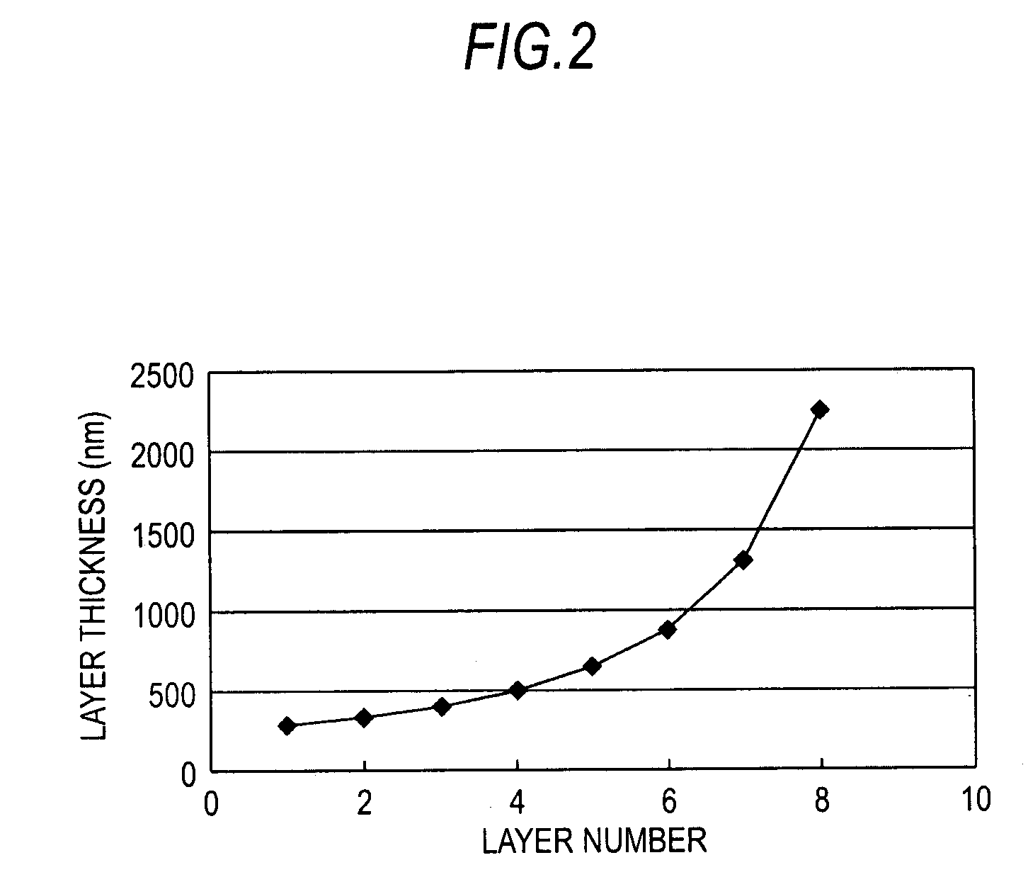
[0086]The buffer layer 60 is a layered structure in which first semiconductor layers 611, . . . , 618 formed of undoped GaN and second semiconductor layers 62, . . . , 62 formed of undoped AlN are alternately formed. A pair of a first semiconductor layer and a neighboring second semiconductor layer being considered as one composite layer, the buffer layer 60 includes eight composite lay...


PUM


Abstract

A semiconductor electronic device comprises a substrate; a buffer layer formed on the substrate, the buffer layer including not less than two layers of composite layer in which a first semiconductor layer formed of a nitride-based compound semiconductor layer having a lattice constant smaller than a lattice constant of the substrate and a thermal expansion coefficient larger than a thermal expansion coefficient of the substrate and a second semiconductor layer formed of a nitride-based compound semiconductor having a lattice constant smaller than a lattice constant of the first semiconductor layer and a thermal expansion coefficient larger than a thermal expansion coefficient of the substrate are alternately laminated; an intermediate layer provided between the substrate and the buffer layer, the intermediate layer being formed of a nitride-based compound semiconductor having a lattice constant smaller than a lattice constant of the first semiconductor layer and a thermal expansion coefficient larger than a thermal expansion coefficient of the substrate; and a semiconductor active layer formed on the buffer layer, the semiconductor active layer being formed of a nitride-based compound semiconductor, wherein: thicknesses of the first semiconductor layers in the buffer layer are non-uniform thereamong, and at least one of the first semiconductor layer has a thickness greater than a critical thickness, the critical thickness being a thickness above which a direction of warp caused by the first semiconductor layer to the substrate is inverted.

Description

CROSS-REFERENCE TO RELATED APPLICATIONS[0001]This application claims priority from Japanese patent application No. 2008-027765 filed on Feb. 7, 2008, and Japanese patent application No. 2008-140649 filed on May 29, 2008, the entire content of which are incorporated herein by reference.BACKGROUND OF THE INVENTION[0002]1. Field of the Invention[0003]The present invention relates to a semiconductor electronic device made of a nitride-based compound semiconductor.[0004]2. Description of the Related Art[0005]The electronic devices such as the field effect transistor or the like using a nitride based compound semiconductor expressed by a formula AlxInyGa1-x-yAsuPvN1-u-v (where 0≦x≦1, 0≦y≦1, x+y≦1, 0≦u≦1, 0≦v≦1, u+v<1), such as a GAN-based compound semiconductor, has attracted a significant attention as a solid state device capable of operating in a high temperature environment close to 400° C. Unlike Si or GaAs, it is difficult to manufacture a large diameter single crystal substrate o...

Claims


Application Information

Patent Timeline
IPC IPC(8): H01L49/02
CPCH01L29/045H01L29/7787H01L29/2003H01L29/155
Inventor KOKAWA, TAKUYAKATO, SADAHIROSATO, YOSHIHIROIWAMI, MASAYUKI
Owner FURUKAWA ELECTRIC CO LTD
Why Eureka
Try Eureka