

Photosensitive resin composition, and, photosensitive element, method for forming resist pattern, method for manufacturing printed wiring board and method for manufacturing partition wall for plasma display panel using the composition
a technology of photosensitive resin and composition, which is applied in the direction of photosensitive materials, electric discharge tubes/lamp manufacture, instruments, etc., can solve problems such as worker safety, and achieve the effect of sufficient sensitivity and resolution
Active Publication Date: 2009-08-13
RESONAC CORP
View PDF12 Cites 7 Cited by
- Summary
- Abstract
- Description
- Claims
- Application Information
AI Technical Summary
Benefits of technology
[0027]According to the invention there are provided a photosensitive resin composition that allows formation of resist patterns with light having a peak in the wavelength range of 350 nm to 440 nm at sufficient sensitivity and resolution, and a photosensitive element, resist pattern forming method, printed circuit board production process and plasma display panel barrier production process using it.
Problems solved by technology
However, mercury lamp light includes ultraviolet rays that are harmful to the human body, and therefore worker safety has been an issue.
Method used
View moreImage
Smart ImageViewing Examples

Examples
examples
[0105]The invention will now be explained in greater detail by examples and comparative examples. This is with the understanding, however, that the invention is not limited to these examples.
Login to View More PUM
 Abstract
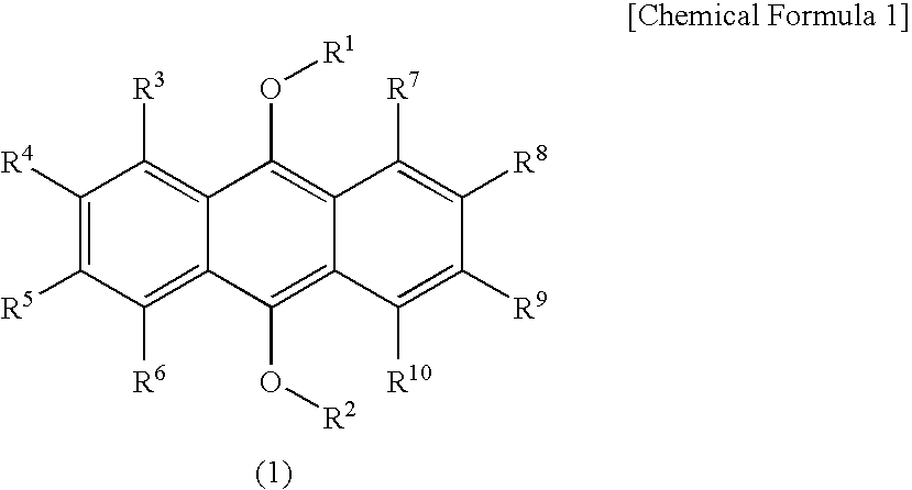
A photosensitive resin composition comprising (A) a binder polymer, (B) a photopolymerizing compound with a polymerizable ethylenic unsaturated bond, (C) a photoradical polymerization initiator containing a 2,4,5-triarylimidazole dimer or its derivative, and (D) a compound represented by the following general formula (1)(wherein R1 and R2 each independently represent C1-20 alkyl, etc., and R3, R4, R5, R6, R7, R8, R9 and R10 each independently represent hydrogen, etc.).
Description
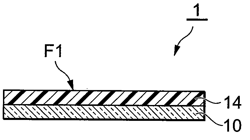
TECHNICAL FIELD[0001]The present invention relates to a photosensitive resin composition, and to a photosensitive element, a resist pattern forming method, a printed circuit board production process and a plasma display panel barrier production process that use it.BACKGROUND ART[0002]Resist materials used for etching or plating with conventional printed circuit board manufacturing technology include widely employed photosensitive elements obtained using photosensitive resin compositions, or the same laminated onto supports and covered with protective films.[0003]For ordinary production of printed circuit boards, first a photosensitive element is stacked (by lamination or the like) onto a circuit-forming board such as a copper board with a layer composed of a photosensitive resin composition (hereinafter referred to as “photosensitive layer”) bonded thereto, and irradiated with active light rays for photocuring (pattern exposure) of prescribed sections of the photosensitive resin com...
Claims
Login to View More Application Information
Patent Timeline
 IPC IPC(8): G03F7/20G03F7/004G03F7/031H01J9/02H01J11/22H01J11/34H01J11/36H05K3/06
CPCG03F7/0007G03F7/029G03F7/031Y10S430/127H01J11/36Y10S430/121H01J9/242G03F7/028
InventorMIYASAKA, MASAHIROKUMAKI, TAKASHI
OwnerRESONAC CORP