Photovoltaic Conversion Element and Manufacturing Method Therefor, and Photovoltaic Conversion Module Using Same
- Summary
- Abstract
- Description
- Claims
- Application Information
AI Technical Summary
Problems solved by technology
Method used
Image

Examples
example 1
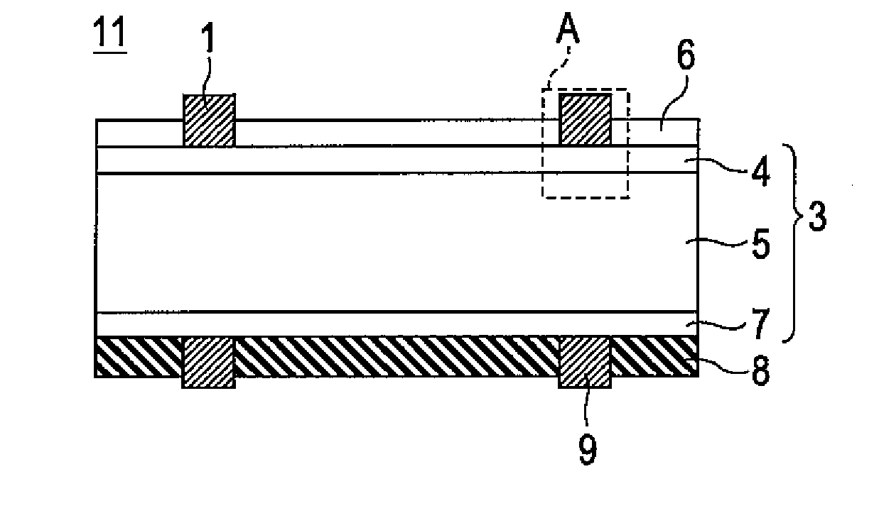
[0232]Description will be made of the experimental results of measurement of a relation between the pn junction oxygen concentration and characteristic of the surface electrodes 1 in a bulk polycrystalline Si solar cell element formed as the photovoltaic conversion element of the present invention according to the above-described embodiment.
[0233]The main conditions for forming the element are as follows: A plate-shaped B-doped p-type polycrystalline Si substrate produced by the cast method and having a resistivity of about 2 Ω·cm, a thickness of about 300 μm, and a size of 150 mm×155 mm was used as the crystalline Si substrate.
[0234]The opposite conductivity-type region 4 was formed by the thermal diffusion method using POCl3 as a diffusion source so that the sheet resistance was 65Ω / □. The surface electrodes 1 were formed by the printing and firing method using Ag paste containing Ag as a main component. The firing was performed by RT treatment using an IR furnace, and the fire-th...
example 2
[0255]A sample of a solar cell element was formed and evaluated by the same method as in Example 1 except that in preparing a polycrystalline silicon ingot by the cast method, the oxygen concentration of a crystal Si substrate before element processing was changed by controlling the degassing time of SiO gas from the surface of a Si melt.
[0256]The results are shown in Table 1.
TABLE 1OxygenOxygenconcentration inconcentrationfirst depletionin substrateregionEfficiencyIscVocYield[atoms / cm3][atoms / cm3][%][A][V]FF[%]1.2E18 1 to 2.0E1815.307.8590.6020.752871.0E18 1 to 1.8E1815.467.8620.6070.753918E171 to 1.6E1815.577.9050.6080.753934E170.9 to 1.1E18 15.727.9510.6090.75595*2E17≦9E1715.907.9960.6110.76198*8E16≦8E1716.027.9980.6110.76298*2E16≦7E1716.028.0020.6110.76298*1E16≦7E1716.058.0030.6110.76398* Samples within the range of the present invention.
[0257]It is confirmed from Table 1 that when the crystalline Si substrate having an oxygen concentration of 2E17 [atoms / cm3] or less is used...
example 3
[0258]The heat treatment step or the laser recrystallization step in the method for manufacturing the photovoltaic conversion element of the present invention was applied to a crystalline Si substrate having an oxygen concentration exceeding 2E17 [atoms / cm3] before element processing to form a low-oxygen-concentration region according to the present invention, followed by element processing.
[0259]The oxygen concentration of the crystalline Si substrate before element processing was kept at 4E17 [atoms / cm3].
[0260]The conditions for the heat treatment step and the laser recrystallization step were as follows:
[Heat Treatment Step]
[0261]The substrate was heat-treated at 1200° C. for 4 minutes at maximum in a hydrogen atmosphere to diffuse oxygen in the substrate to the outside and form a region having an oxygen concentration of 2E17 [atoms / cm3] or less to a depth of about 1.5 μm at maximum (under the conditions of 1200° C. and 4 minutes) from the substrate surface.
[0262]The depth was de...
PUM
 Abstract
Description
Claims
Application Information
 - R&D Engineer
- R&D Manager
- IP Professional
- Industry Leading Data Capabilities
- Powerful AI technology
- Patent DNA Extraction
Browse by: Latest US Patents, China's latest patents, Technical Efficacy Thesaurus, Application Domain, Technology Topic.
© 2024 PatSnap. All rights reserved.Legal|Privacy policy|Modern Slavery Act Transparency Statement|Sitemap