Nanostructure-Based Electronic Device

Inactive Publication Date: 2009-08-27
AGILENT TECH INC
View PDF0 Cites 8 Cited by
  • Summary
  • Abstract
  • Description
  • Claims
  • Application Information

AI Technical Summary

Problems solved by technology

However, this process is complicated and, in practice, is still somewhat random because it does not effectively control the orientation of the CNTs grown from the catalyst.
In addition, the CVD growth method does not control the chirality (handedness) of the CNTs grown using this process.
While this method is elegant, to use in a practical application, it requires that the dsDNA be located on the substrate with an accuracy that is difficult to achieve in practice.
This allows precise placement of CNTs on the surface, but the gold surface does not allow bottom-gate CNT FETs to be formed.
Nor does the gold surface easily allow multiple aligned mask layers to be used to fabricate more complicated gate CNTFET structures.
The process precisely defines the locations of CNTs on the surface of a substrate, but does not provide electrodes that make electrical contact with the ends of the CNTs so that the CNTs may constitute parts of respective electronic devices, such as CNT FETs.

Method used


Image

  • Nanostructure-Based Electronic Device
  • Nanostructure-Based Electronic Device
  • Nanostructure-Based Electronic Device

Examples


Embodiment Construction

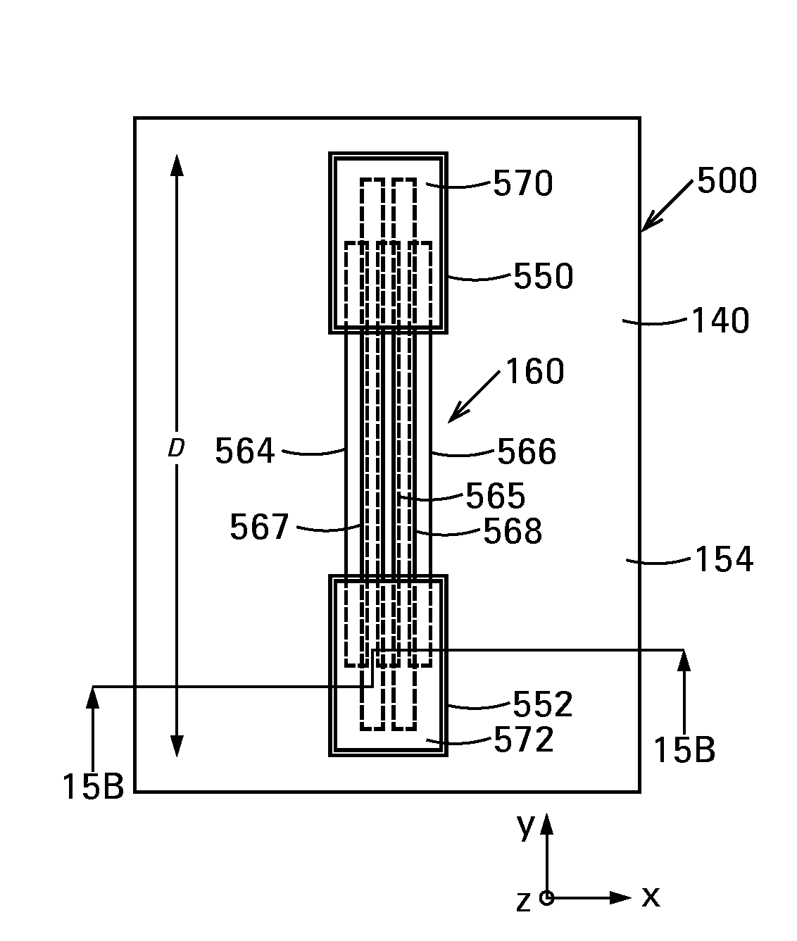
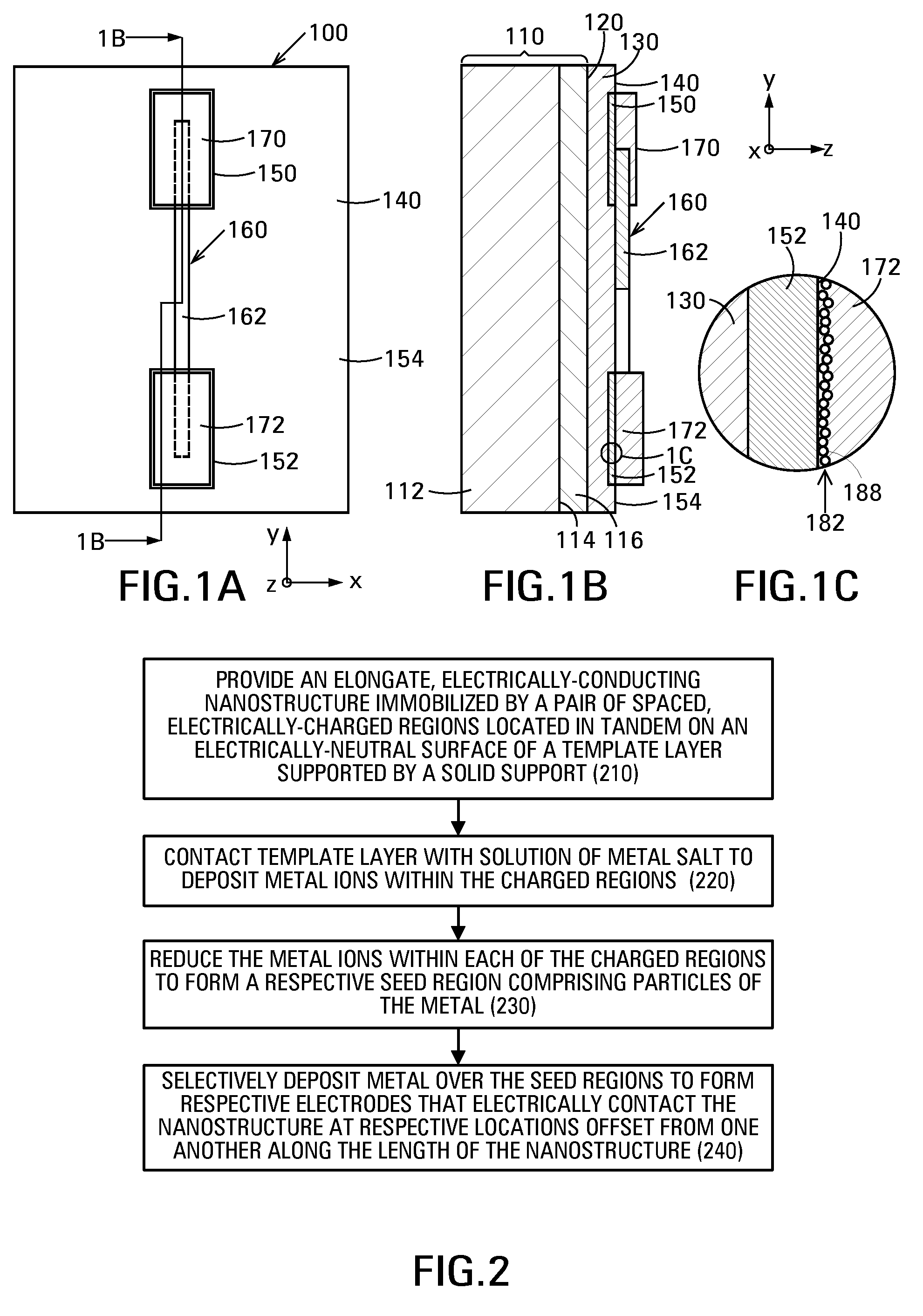
[0021]Embodiments of the invention provide a nanostructure-based electronic device, such as a carbon nanotube field-effect transistor (CNTFET), that comprises a solid support having a support surface, and an organic template layer on the support surface. The template layer has a surface comprising a pair of spaced, electrically-charged regions arranged in tandem in an electrically-neutral background. The electronic device additionally comprises an elongate, electrically-conducting nanostructure extending between the charged regions, and electrodes on the surface of the template layer at least co-extensive with the charged regions and in electrical contact with the nanostructure.

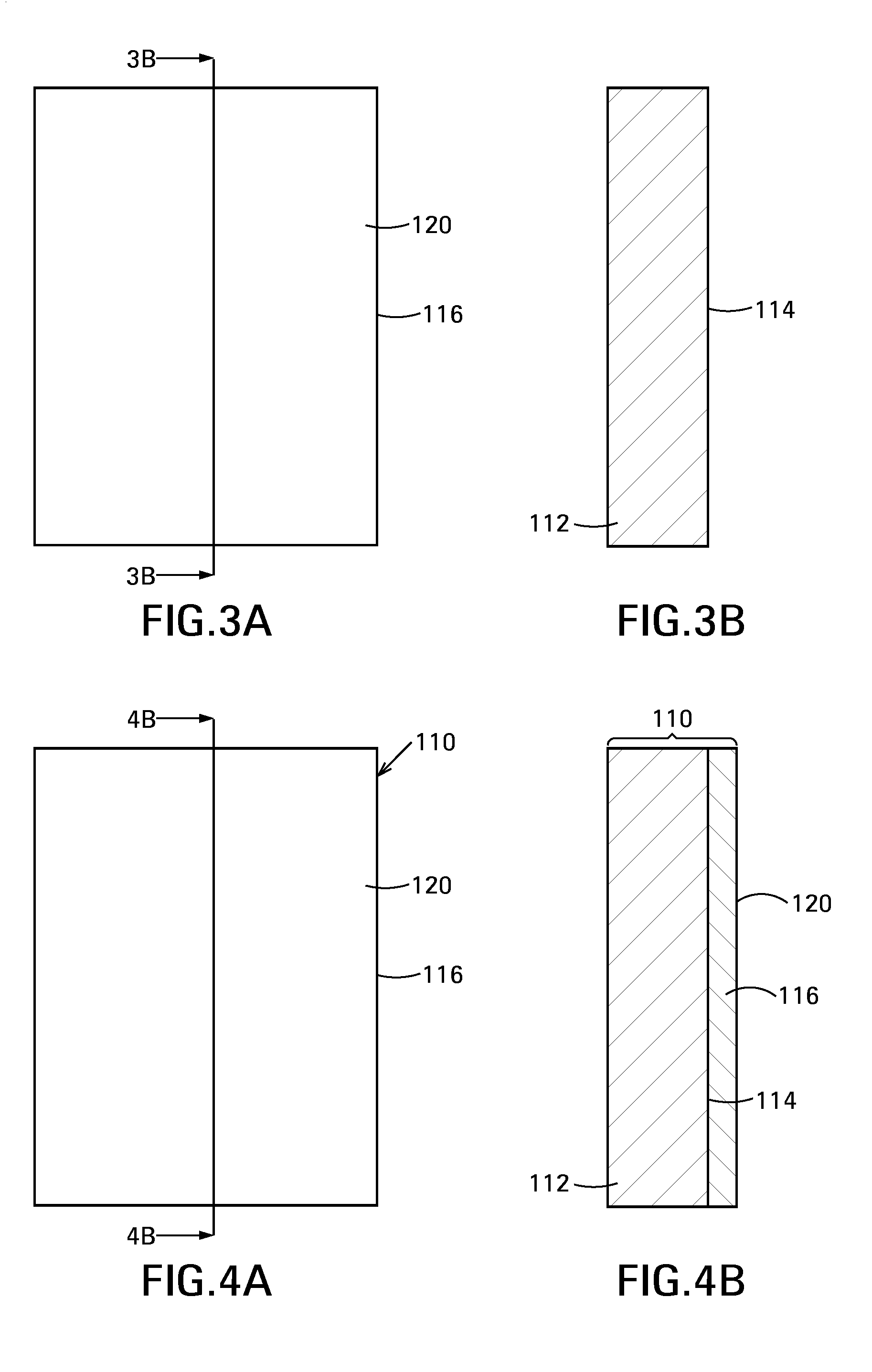
[0022]FIGS. 1A and 1B are respectively a plan view and a cross-sectional view showing an example of a nanostructure-based electronic device 100 in accordance with an embodiment of the invention. Electronic device 100 is composed of a solid support 110 having a support surface 120. An organic template layer 13...


PUM


Abstract

The nanostructure-based electronic device comprises a solid support, an organic template layer, a nanostructure and electrodes. The organic template layer is on the surface of the solid support, and has a surface comprising a pair of spaced, electrically-charged regions arranged in tandem in an electrically-neutral background. The nanostructure is elongate, is electrically-conducting, and extends between the charged regions. The electrodes are located the surface of the template layer and are at least co-extensive with the charged regions.

Description

BACKGROUND[0001]Two basic approaches are used to manufacture nanostructure-based electronic devices. A top-down method, which is similar to that used for making integrated circuits, transfers patterns to a substrate using photolithography, and additionally involves material deposition and etching. A bottom-up method fabricates nanostructures, ideally molecule-by-molecule, or even atom-by-atom. Many advanced techniques have been developed to make many kinds of nanostructures, including single or multiple nanoparticles, nanotubes, nanowires, nanoribbons, etc. of various materials.[0002]Carbon nanotubes (CNTs) have attracted much attention recently due to their impressive mechanical, electrical and optical properties. Extensive studies have been conducted on CNTs, especially on CNT-based field-effect-transistors (CNT FETs). However the difficulty of precisely locating the CNTs on a substrate and of making electrical connections to the CNTs is still a substantial obstacle to large-scale...

Claims


Application Information

Patent Timeline
IPC IPC(8): H01L21/283H01L29/12
CPCB82Y10/00H01L21/76895H01L2221/1094H01L51/055H01L51/0558H01L51/0048H10K85/221H10K10/481H10K10/484
Inventor LIU, MAOZIKOPLEY, THOMAS E.ROSNER, S. JEFFREY
Owner AGILENT TECH INC
Why Eureka
Try Eureka