Super hybrid soi CMOS devices

a technology of cmos and super hybrids, applied in the field of high-performance semiconductor devices, can solve the problems of significant deformation of electron mobility on (b>110/b>) si surfaces, inability to meet the requirements of nfet devices, and undesirable pfets with larger widths

Inactive Publication Date: 2009-08-27
INT BUSINESS MASCH CORP
View PDF15 Cites 20 Cited by
  • Summary
  • Abstract
  • Description
  • Claims
  • Application Information

AI Technical Summary

Benefits of technology

[0013]The present invention provides semiconductor structures comprised of stressed channels (including uni-axial and / or bi-axial strained channels) on hybrid oriented surfaces on a homogeneous SOI substrate instead of a mixed substrate with SOI and bulk, wherein the combined technologies provide a synergistic improvement in carrier mobility as well as a method of fabricating the inventive semiconductor structures.
[0015]The semiconductor structures of the present invention include at least one trench isolation region that separates CMOS devices having different polarities from each other. That is, a trench isolation region including a trench dielectric material is typically present between an nFET and a pFET. The trench isolation region employed in the present invention has a region laterally abutting the active area of one of the semiconductor devices in which at least a portion thereof has been removed and filled with a dielectric material that has a lower stress value as compared to that of a conventional trench dielectric material and as such the entire stress value of the trench isolation region is lowered. In the present invention, the dielectric material present in the region that laterally abuts the active area of one of the semiconductor devices is different from that of the trench dielectric material.

Problems solved by technology

To compensate for this discrepancy, pFETs are typically designed with larger widths in order to balance pull-up currents against the nFET pull-down currents and achieve uniform circuit switching. pFETs having larger widths are undesirable since they take up a significant amount of chip area.
Unfortunately, electron mobility on (110) Si surfaces is significantly degraded compared to (100) Si surfaces.
As can be deduced from the above, the (110) Si surface is optimal for pFET devices because of excellent hole mobility, yet such a crystal orientation is completely inappropriate for nFET devices.

Method used


Image

  • Super hybrid soi CMOS devices
  • Super hybrid soi CMOS devices
  • Super hybrid soi CMOS devices

Examples


Embodiment Construction

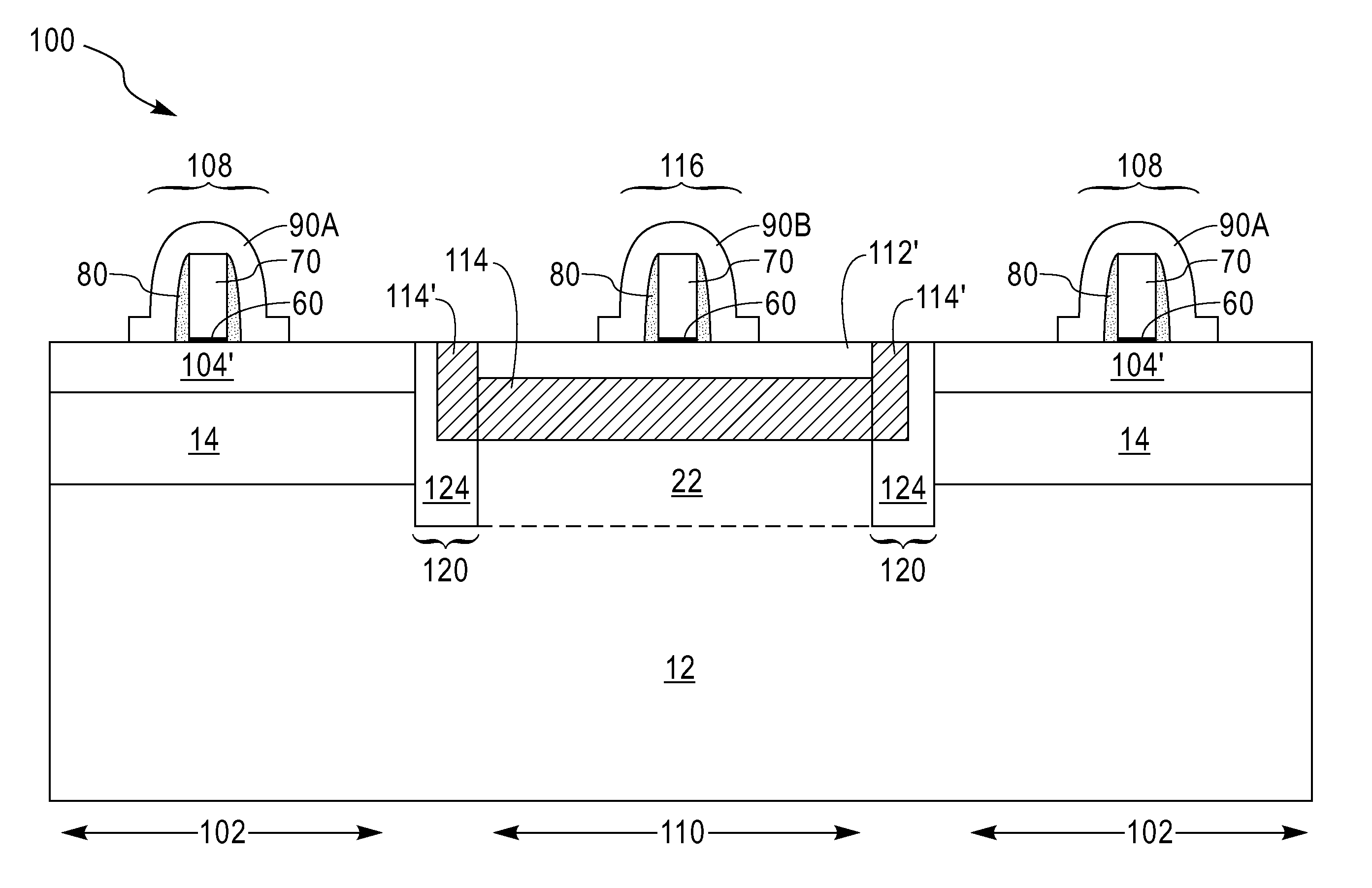
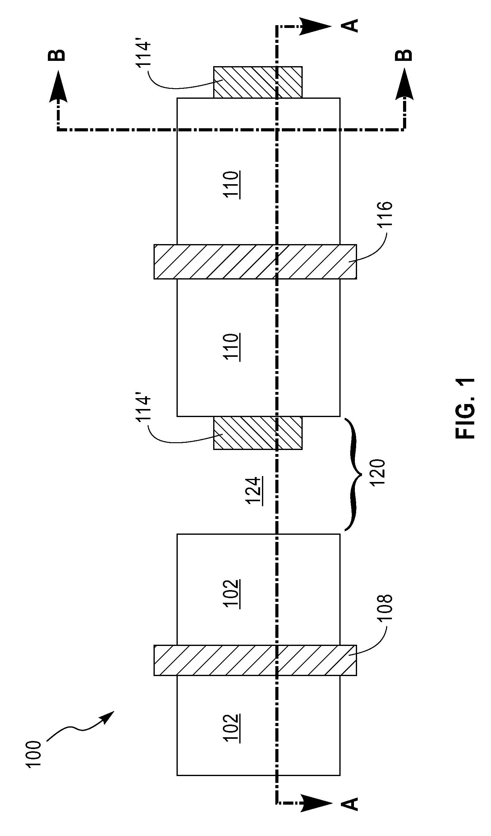
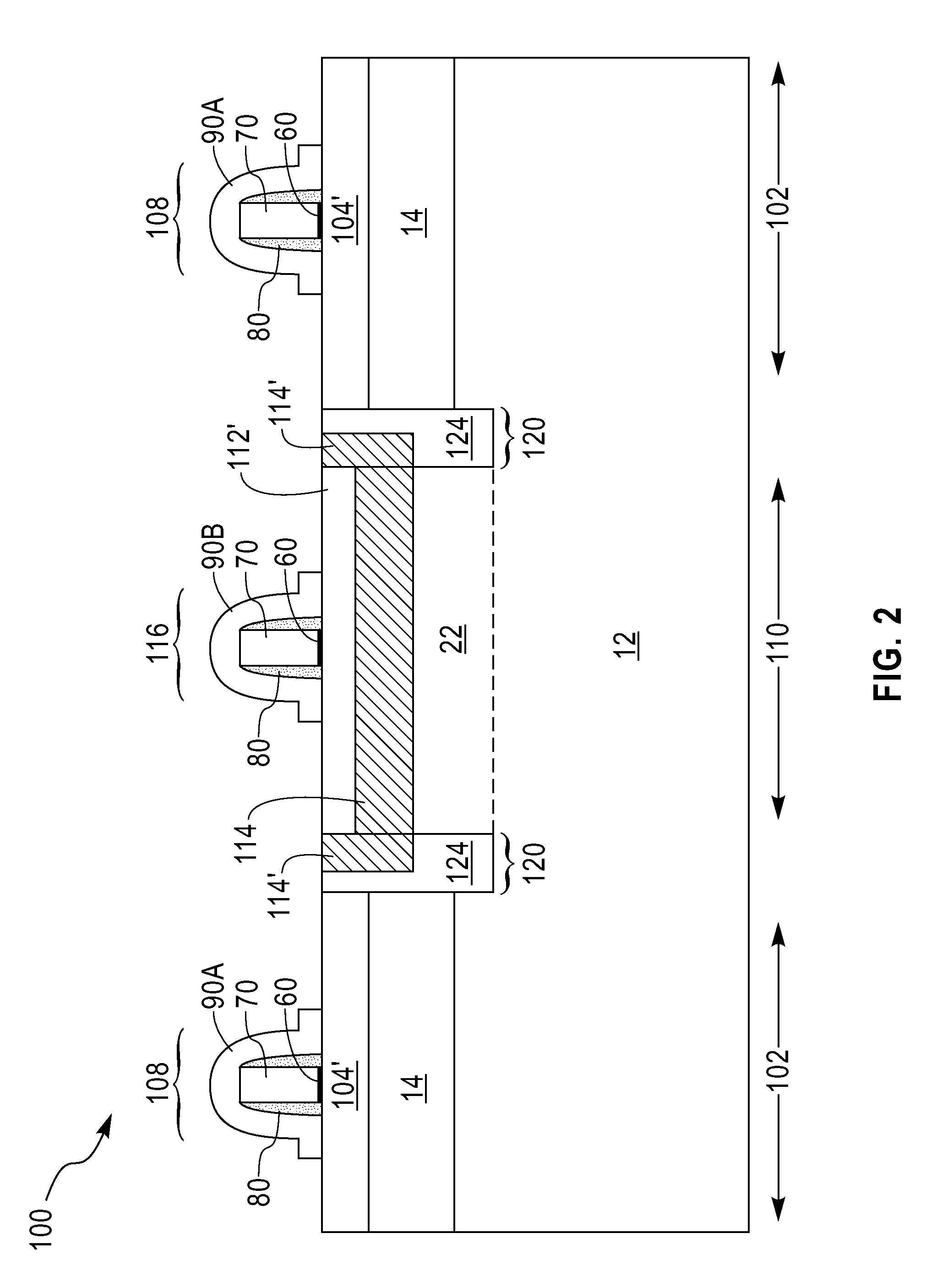
[0031]The present invention, which provides semiconductor structures including stressed channels on a hybrid oriented substrate as well as a method of fabricating the same, will now be described in greater detail by referring to the drawings that accompany the present application. It is noted that the drawings of the present application are provided for illustrative purposes and thus they are not drawn to scale. Moreover, in the drawings, like reference numerals are used in describing like and / or corresponding elements.

[0032]In the following description, numerous specific details are set forth, such as particular structures, components, materials, dimensions, processing steps and techniques, in order to provide a thorough understanding of the present invention. However, it will be appreciated by one of ordinary skill in the art that the invention may be practiced without these specific details. In other instances, well-known structures or processing steps have not been described in ...


PUM


Abstract

The present invention provides semiconductor structures comprised of stressed channels on hybrid oriented. In particular, the semiconductor structures include a first active area having a first stressed semiconductor surface layer of a first crystallographic orientation located on a surface of a buried insulating material and a second active area having a second stressed semiconductor surface layer of a second crystallographic orientation located on a surface of a dielectric material. A trench isolation region is located between the first and second active area, and the trench isolation region is partially filled with a trench dielectric material and the dielectric material that is present underneath said second stressed semiconductor surface layer. The dielectric material within the trench isolation region has lower stress compared to that is used in conventional STI process and it is laterally abuts at least the second stressed semiconductor surface layer and extends to an upper surface of the trench isolation region.

Description

RELATED APPLICATION[0001]This application is a divisional of U.S. patent application Ser. No. 11 / 758,454, filed Jun. 5, 2007.FIELD OF THE INVENTION[0002]The present invention relates to high-performance semiconductor devices for digital or analog applications, and more particularly to complementary metal oxide semiconductor (CMOS) devices that have mobility enhancement from stress and surface orientation. Specifically, the present invention provides stressed CMOS devices that are located on a hybrid orientated substrate.BACKGROUND OF THE INVENTION[0003]In present semiconductor technology, CMOS devices, such as nFETs or pFETs, are typically fabricated upon semiconductor wafers, such as Si, that have a single crystal orientation. In particular, most of today's semiconductor devices are built upon Si having a (100) crystal orientation.[0004]Electrons are known to have a high mobility for a (100) Si surface orientation, but holes are known to have a high mobility for a (110) surface ori...

Claims


Application Information

Patent Timeline
Patent Type & Authority Applications(United States)
IPC IPC(8): H01L29/04
CPCH01L21/823807H01L21/823878H01L27/1207H01L27/1203H01L29/7843H01L21/84
Inventor IEONG, MEIKEIOUYANG, QIQING C.
Owner INT BUSINESS MASCH CORP
Why Eureka
Try Eureka