Three-Dimensional Direct-Write Lithography

a lithography and three-dimensional technology, applied in the field of three-dimensional direct-write lithography, can solve the problems of 3d structure, large, expensive and limited complexity, and implementation devices encapsulated by a single material system,

Inactive Publication Date: 2009-09-03
UNIV OF COLORADO THE REGENTS OF
View PDF8 Cites 40 Cited by
  • Summary
  • Abstract
  • Description
  • Claims
  • Application Information

AI Technical Summary

Benefits of technology

[0009]Embodiments of the present invention provide a method of creating a region of index change in a photopolymer. The method includes providing a photopolymer having a photosensitivity to light of a particular wavelength and creating a region of index change in the photopolymer by applying direct write lithography to expose the photopolymer of the region to light that includes the particular wavelength. The region of index change may be a localized mark of index change or a trajectory through space. A cross section of the region of index change may vary along the trajectory. The region of index change may be a two-dimensional pattern of index change having substantially no variation in a third dimension. The region of index change may be a three-dimensional pattern of index change. The region of index change may be an optical device. The optical device may be a lens, a waveguide, a grating, a prism, and / or the like. The method my include providing a dopant doped into the photopolymer. The method may include exposing the photopolymer to uniform incoherent light to thereby cure the polymer.

Problems solved by technology

The results are typically unreliable, large, expensive and of limited complexity due to the moderate individual yield.
Traditional planar lightwave circuits can fabricate complex optical interconnections but are generally unable to incorporate hybrid subcomponents and thus can only implement devices encompassed by a single material system.
An alternative approach is to reduce the scale of the “scaffold” via lithographic silicon micro-machining, but the precise and identical nature of each silicon bench demands similar tolerances for the subcomponents that are not economically feasible.
This material process is not compatible with deeply buried, 3D structures.
Only limited functionality can be attained by this method since the hybridized components must be thin (to minimize diffraction losses within the part) and optically flat to much less than a wavelength (to minimize coupling losses).
This technique has limited control over the shape and direction of the resulting waveguides, and single mode operation has not yet been demonstrated over a significant distance.

Method used


Image

  • Three-Dimensional Direct-Write Lithography
  • Three-Dimensional Direct-Write Lithography
  • Three-Dimensional Direct-Write Lithography

Examples


embodiment

Exemplary Method Embodiment

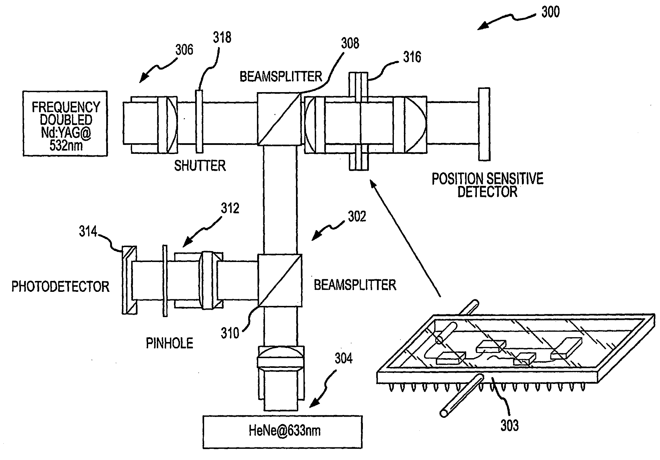
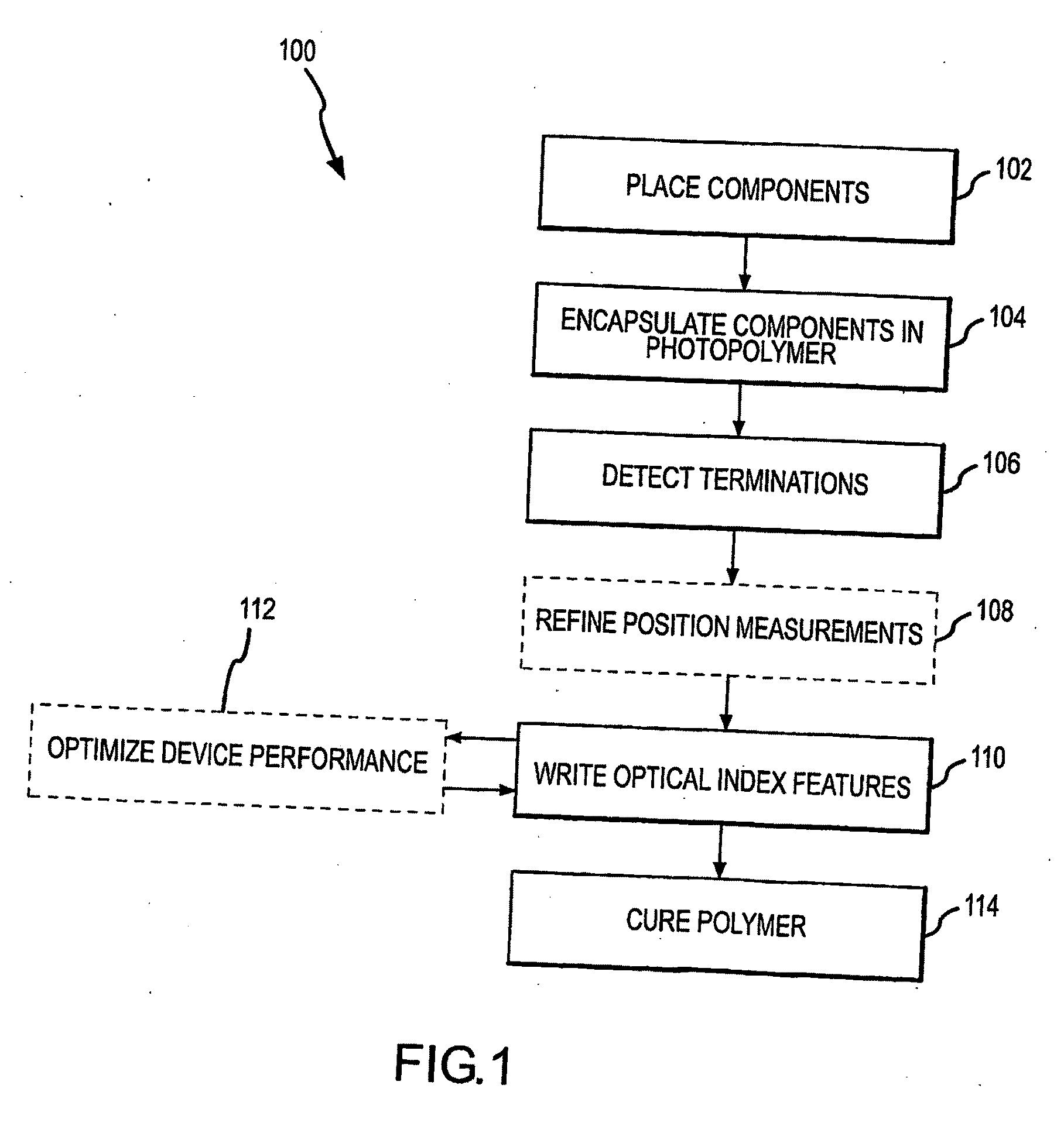
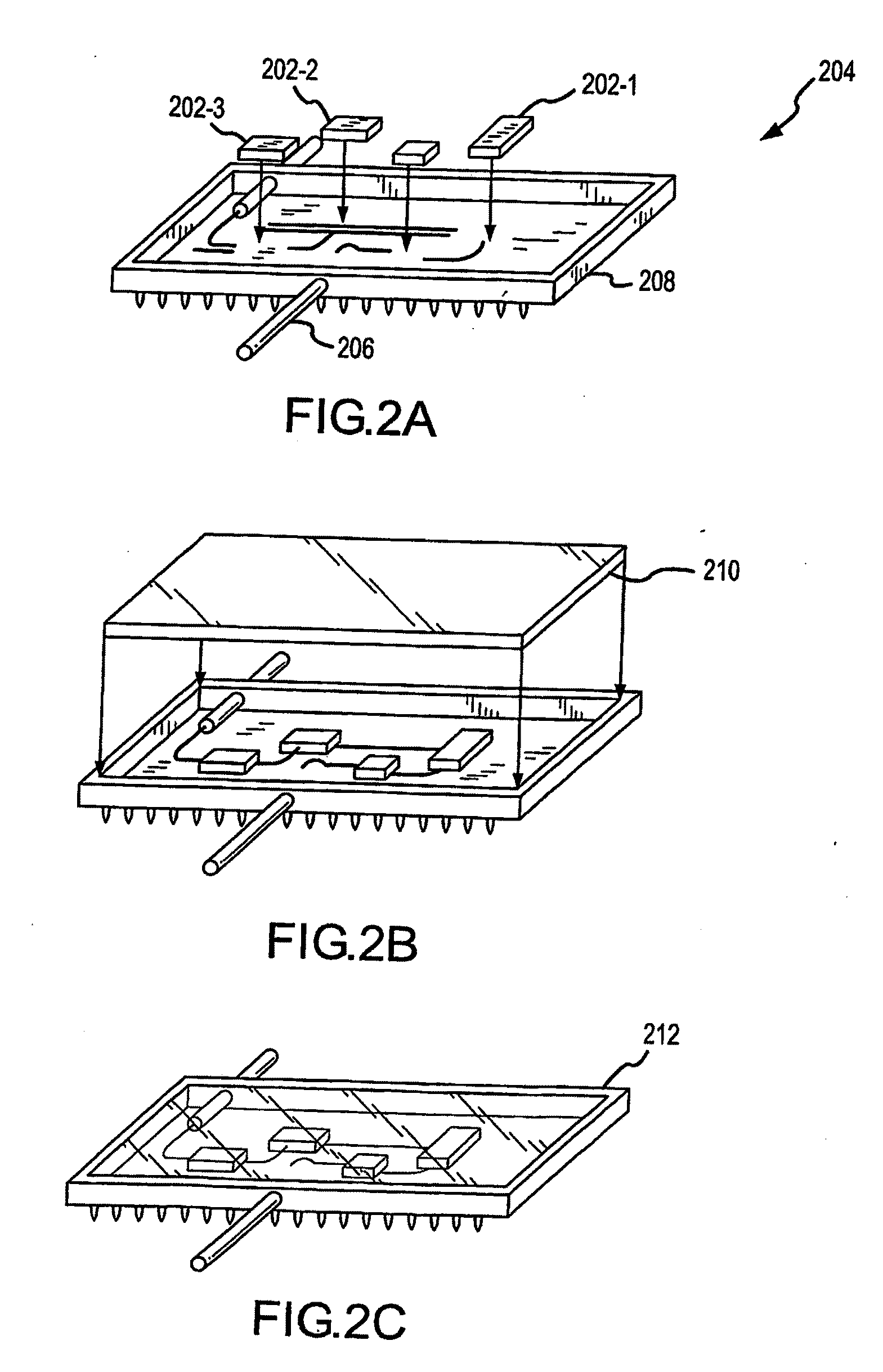
[0029]Having described embodiments of the present invention generally, attention is directed to FIG. 1, which illustrates an exemplary method 100 according to embodiments of the invention. The method relates to direct write lithography into a diffusion-mediated photopolymer. Those skilled in the art will appreciate that this method is not limiting. There are other methods of creating local, permanent index change in polymers, such as two-photon initiation. Those skilled in the art also will appreciate that the method 100 is merely exemplary of a number of methods according to the present invention. For example, the foregoing description is specifically directed toward forming a waveguide connecting optical components, although this is not to be considered limiting. Further, those skilled in the art also will appreciate that other methods according to other embodiments may include more, fewer, or different steps than those illustrated herein. Further still,...


PUM

PropertyMeasurementUnit
output poweraaaaaaaaaa
speedaaaaaaaaaa
speedsaaaaaaaaaa

Abstract

A method of creating a region of index change in a photopolymer includes providing a photopolymer having a photosensitivity to light of a particular wavelength and creating a region of index change in the photopolymer by applying direct write lithography to expose the photopolymer of the region to light that includes the particular wavelength.

Description

CROSS-REFERENCES TO RELATED APPLICATIONS[0001]This application is a non-provisional of and claims the benefit of co-pending, commonly assigned U.S. Provisional Patent Application No. 60 / 691,471, filed on Jun. 18, 2005, entitled “HYBRID INTEGRATED PHOTONICS,” then entirety of which is herein incorporated by reference for all purposes.[0002]This application is related to co-pending, commonly assigned U.S. patent application Ser. No. 11 / 357,737, entitled “MONOLITHIC WAVEGUIDE ARRAYS,” then entirety of which is herein incorporated by reference for all purposes.BACKGROUND OF THE INVENTION[0003]This application relates generally to optical packaging systems and methods. More specifically, this application relates to optical packaging and circuit fabrication systems and methods using three-dimensional, direct-write lithography.[0004]Present optical packaging systems are a direct descendant of gun sights developed in WW II in which optics are manually aligned and then epoxied to machined me...

Claims


Application Information

Patent Timeline
Patent Type & Authority Applications(United States)
IPC IPC(8): A61N5/00
CPCG03F7/70416B29C59/16G03F7/2053G02B6/12002G02B6/12G03F7/70025B29C2035/0838
Inventor MCLEOD, ROBERT R.
Owner UNIV OF COLORADO THE REGENTS OF
Why Eureka
Try Eureka