
Polishing compound for semiconductor wafer polishing and polishing method

a technology of polishing compound and semiconductor wafer, which is applied in the direction of lapping machine, manufacturing tools, other chemical processes, etc., to achieve the effect of small change in polishing rate according to concentration chang

Inactive Publication Date: 2009-09-10
NIPPON CHECMICAL IND CO LTD +1
View PDF3 Cites 49 Cited by
  • Summary
  • Abstract
  • Description
  • Claims
  • Application Information

AI Technical Summary

Benefits of technology

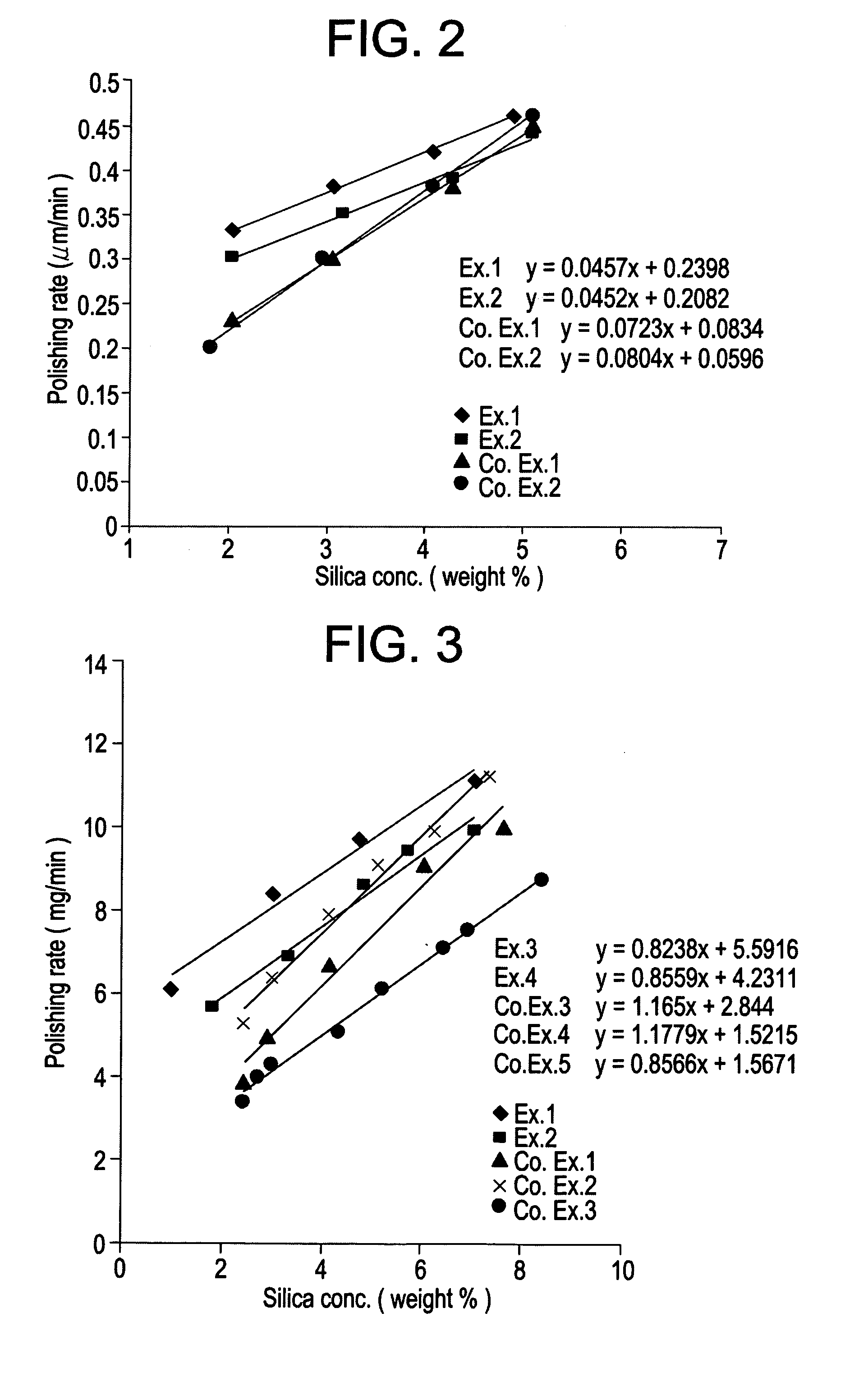
[0024]Therefore, the object of the present invention is to provide a polishing compound of lower alkali metal contents for semiconductor wafer polishing characterized to have high polishing rate and change of polishing rate according to change of concentration is small. And, another object of the present invention is to provide a method for polishing of semiconductor wafer using said polishing compound.

Problems solved by technology

At this washing process, remain of abrasive particles on the surface of wafer is pointed out as a problem, and it is considered that alkali metal, especially sodium, takes part to the mechanism of remain of abrasive particles.
This problem can be improved largely by changing polishing condition or washing method, however, since these changes accompany remarkable deterioration of polishing rate or complication of washing method, these changes have not dissolve the problem.

Method used


Image

  • Polishing compound for semiconductor wafer polishing and polishing method
  • Polishing compound for semiconductor wafer polishing and polishing method

Examples


preparation example 1

[0093]520 g of JIS 3 sodium silicate (SiO2: 28.8 weight %, Na2O: 9.7 weight %, H2O: 61.5 weight %) is added to 2810 g of deionized water, mixed homogeneously and diluted sodium silicate of silica concentration 4.5 weight % is prepared. This diluted sodium silicate is passed through a column containing 1200 mL of H type strong acidic cation exchange resin (AMBERLITE IR120B, product of ORGANO CORPORATION), which is previously regenerated by hydrochloric acid and dealkalized, then 4040 g of active silicic acid characterized that silica concentration is 3.7 weight % and pH is 2.9 is obtained.

[0094]Then, colloidal particles are grown up by a build up method. That is, to 500 g of said obtained active silicic acid, 20 weight % TEAOH aqueous solution is added by stirring and pH is adjusted to 9, heated to 90° C. to boiling point and preserved for 1 hour, then remaining 3540 g of active silicic acid is added by 6 hours. During adding process, 20 weight % TEAOH aqueous solution is added so as...

preparation example 2

[0095]520 g of JIS 3 sodium silicate (SiO2: 28.8 weight %, Na2O: 9.7 weight %, H2O: 61.5 weight %) is added to 2810 g of deionized water, mixed homogeneously and diluted sodium silicate of silica concentration 4.5 weight % is prepared. This diluted sodium silicate is passed through a column containing 1200 mL of H type strong acidic cation exchange resin (AMBERLITE IR120B, product of ORGANO CORPORATION), which is previously regenerated by hydrochloric acid and dealkalized, then 4040 g of active silicic acid characterized that silica concentration is 3.7 weight % and pH is 2.9 is obtained.

[0096]Then, colloidal particles are grown up by a build up method. That is, to 500 g of said obtained active silicic acid, equimolar mixture of 20 weight % TEAOH aqueous solution and 25 weight % TMAOH aqueous solution is added by stirring and pH is adjusted to 9, heated to 90° C. to boiling point and preserved for 1 hour, then remaining 3540 g of active silicic acid is added by 6 hours. During addin...

preparation example 3

[0097]520 g of JIS 3 sodium silicate (SiO2: 28.8 weight %, Na2O: 9.7 weight %, H2O: 61.5 weight %) is added to 2810 g of deionized water, mixed homogeneously and diluted sodium silicate of silica concentration 4.5 weight % is prepared. This diluted sodium silicate is passed through a column containing 1200 mL of H type strong acidic cation exchange resin (AMBERLITE IR120B, product of ORGANO CORPORATION), which is previously regenerated by hydrochloric acid and dealkalized, then 4040 g of active silicic acid characterized that silica concentration is 3.7 weight % and pH is 2.9 is obtained.

[0098]Then, colloidal particles are grown up by a build up method. That is, to 500 g of said obtained active silicic acid, 25 weight % TMAOH aqueous solution is added by stirring and pH is adjusted to 9, heated to 90° C. to boiling point and preserved for 1 hour, then remaining 3540 g of active silicic acid is added by 6 hours. During adding process, 20 weight % TEAOH aqueous solution is added so as...


PUM

PropertyMeasurementUnit
molar ratioaaaaaaaaaa
pHaaaaaaaaaa
particle sizeaaaaaaaaaa

Abstract

The polishing compound for semiconductor wafer of the present invention contains colloidal silica composed of silica particles to which tetraethylammonium is fixed, and concentration of silica particles dispersed in water is between 0.5 to 50 weight %. Concentration of tetraethylammonium contained in silica particles to which tetraethylammonium is fixed is desirable to be in the range from 5x10⁻⁴ to 2.5x10⁻² as indicated by molar ratio of tetraethylammonium / silica.

Description

FIELD OF THE INVENTION[0001]The present invention relates to a polishing compound that polishes the surface or edge part of a semiconductor wafer such as silicon wafer or semiconductor device substrate on the surface of which metal film, oxide film or nitride film (hereinafter shortened to metal films) is formed. Further, the present invention relates to a method for polishing of the surface or edge part of a semiconductor wafer using this polishing compound.DESCRIPTION OF THE PRIOR ART[0002]Regarding a polishing compound that polishes the surface or edge part of a semiconductor wafer such as silicon wafer or semiconductor device substrate on the surface of which metal films is formed, many kinds of compounds are proposed. As a polishing compound that is mainly composed of silica abrasives, solution containing alkaline component is popular, and the theory for polishing can be explained as follows. That is, chemical action by alkaline component, specifically, erosive action of alkali...

Claims


Application Information

Patent Timeline
Patent Type & Authority Applications(United States)
IPC IPC(8): C09K3/14B24B37/00H01L21/304
CPCC09G1/02H01L21/30625C09K3/1463
Inventor NAKAJO, MASARUIZUMI, MASAHIROMIYABE, SHINSUKEMAEJIMA, KUNIAKITANAKA, HIROAKI
Owner NIPPON CHECMICAL IND CO LTD
Learn More