Flourescence detecting method and fluorescence detecting apparatus

a fluorescence detection and fluorescence technology, applied in the direction of luminescent dosimeters, optical radiation measurement, instruments, etc., can solve the problems of poor reproducibility, difficult to completely uniformize all of the factors for each measurement, and low cost. achieve the effect of low cos

Active Publication Date: 2009-10-01
FUJIFILM CORP
View PDF4 Cites 11 Cited by
  • Summary
  • Abstract
  • Description
  • Claims
  • Application Information

AI Technical Summary

Benefits of technology

[0015]The present invention has been developed in view of the aforementioned problem. It is an object of the present invention to provide a fluorescence detecting method and a fluorescence detecting apparatus that can realize measurements having reproducibility, in which fluctuations in intensities of electric field enhancing fields that occur at each measurement are suppressed, simply and at low cost.
[0026]Here, the term “electric field enhancing field” refers to a local region on the upper surface of the metal film that exhibits an enhancing effect of electric fields, generated due to the evanescent waves which are generated by irradiating the excitation light beam onto the interface between the dielectric plate and the metal film such that conditions for total reflection are satisfied at the interface, and due to surface plasmon which are induced by the evanescent waves and generated within the metal film.
[0039]In the fluorescence detecting method and the fluorescence detecting apparatus of the present invention, the intensity of fluorescence detected in each measurement is corrected based on the intensity of the scattered light of the second electric field enhancing field, which is generated by irradiation of the reference light beam having a longer wavelength than the excitation light beam. The intensity of fluorescence and the intensity of scattered light are both dependent on the generated state of the first electric field enhancing field and the second electric field enhancing field. In addition, the generated state of the electric field enhancing field is dependent on the measurement environment. Accordingly, the scattered light, the intensity of which is substantially proportionate to the intensity of the first electric field enhancing field and the second electric field enhancing field, is employed as an index of the generated state of the first electric field enhancing field and the second electric field enhancing field. Thereby, the intensity of the first electric field enhancing field can be estimated from the relationships between the intensity of the first electric field enhancing field and the intensity of the second electric field enhancing field. Thereby, it becomes possible to normalize and correct the intensity of fluorescence with respect to the intensity of the first electric field enhancing field.
[0040]As described above, correction suited to conditions can be performed for each measurement, and the factors that contribute to fluctuations in the intensity of the electric field enhancing effect that occur during each measurement can be suppressed. Accordingly, measurements having reproducibility can be realized simply and at low cost, without selecting or exchanging components to be optimal for each measurement.

Problems solved by technology

Therefore, it is difficult to completely uniformize all of the factors for each measurement.
This causes a problem that detected intensities of fluorescence fluctuate, and that reproducibility is poor, even if the amounts of detection target substances within samples are the same.
These factors include: margins of error in the shapes and settings of sensor chips; shifting in the incident angle of excitation light beams caused by human error such as margins of errors in sensing and margins of error in setup of the optical system; and shifting in surface plasmon generating conditions due to physical factors such as the refractive indices of samples, the refractive indices of the sensor chips, irregularities on the surfaces of the sensor chips, the thicknesses of the metal films, and the densities of the metal films.
In addition, changes in environmental temperatures during measurement may also lead to shifting in the aforementioned conditions, and therefore must be considered as well.
However, extreme amounts of trouble and cost will be incurred if variations in all of the factors are suppressed by selecting or exchanging components.

Method used


Image

  • Flourescence detecting method and fluorescence detecting apparatus
  • Flourescence detecting method and fluorescence detecting apparatus
  • Flourescence detecting method and fluorescence detecting apparatus

Examples


first embodiment

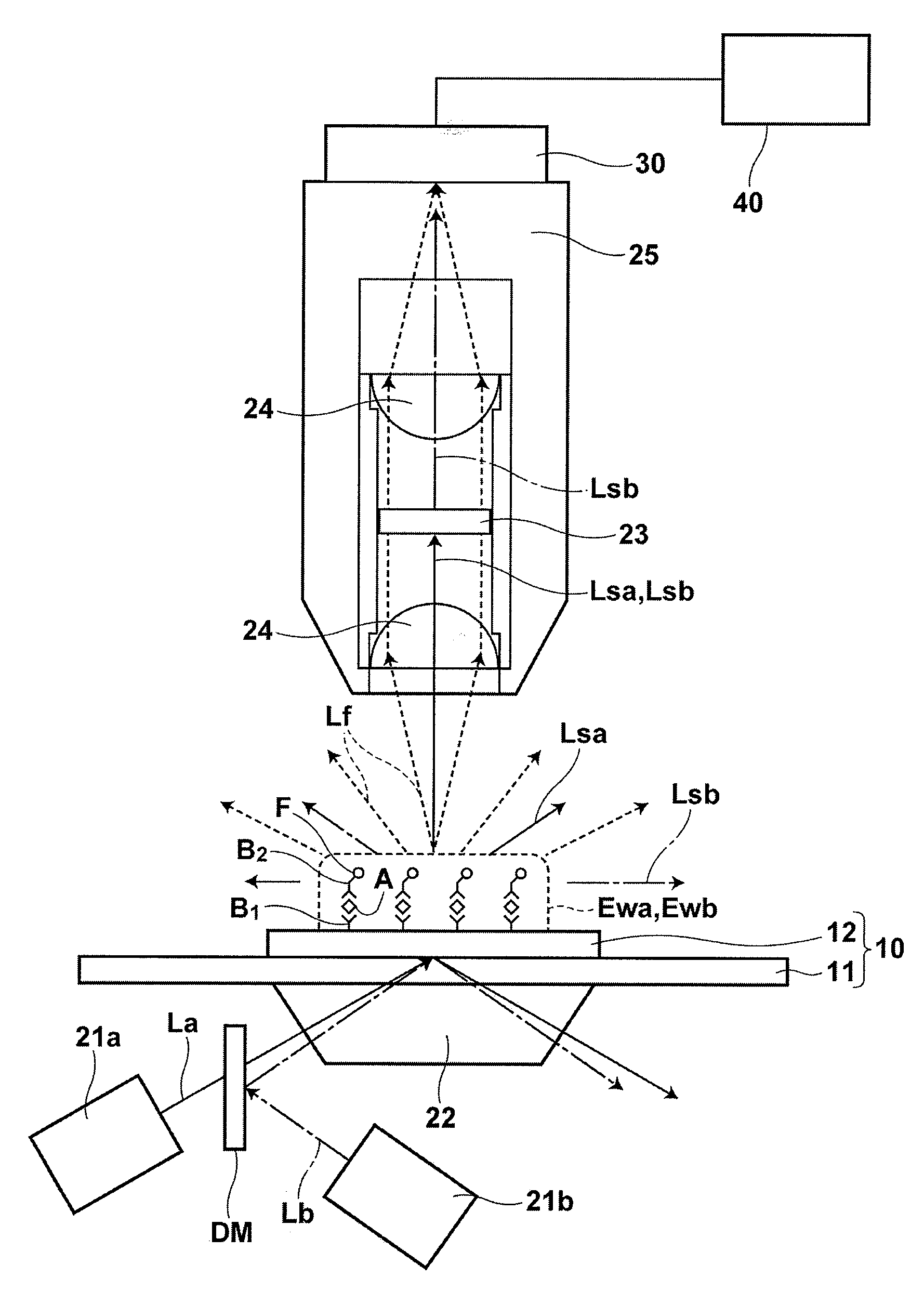
[0049]FIG. 1 is a schematic diagram that illustrates a fluorescence detecting apparatus according to a first embodiment of the present invention.

[0050]As illustrated in FIG. 1, the fluorescence detecting apparatus is equipped with: a sensor chip 10 constituted by a dielectric plate 11 and a metal film 12; a light source 21a that emits an excitation light beam La having a wavelength of 657 nm that excites fluorescent labels F; a light source 21b that emits a reference light beam Lb having a wavelength of 670 nm, which is longer than the wavelength of the excitation light beam La; a prism 22, on which the sensor chip 10 is placed; an optical system DM for guiding the reference light beam Lb such that it passes through the prism 22 and enters the interface between the dielectric plate 11 and the metal film 12 such that a second electric field enhancing field Ewb is generated on the metal film 12; a photodetector 30 for detecting fluorescence Lf emitted by the fluorescent labels F which...

second embodiment

[0083]A second embodiment of the present invention differs from the first embodiment only in that the wavelength of a reference light beam Lb is 780 nm, an excitation light beam La and the reference light beam Lb are emitted simultaneously, and two photodetectors are employed. Accordingly, descriptions of components of the second embodiment which are the same as those of the first embodiment will be omitted insofar as they are not particularly necessary.

[0084]As illustrated in FIG. 4, a fluorescence detecting apparatus according to the second embodiment of the present invention is the fluorescence detecting apparatus according to the first embodiment illustrated in FIG. 1, with a dichroic mirror 23′ provided between the two planoconvex lenses 24 and toward the side of the optical filter 23 from which light enters, and a second photodetector 30b. Note that the second photodetector 30b is connected to the correction calculating mechanism 40 so as to transmit detected light signals the...


PUM


Abstract

An excitation light beam of a wavelength that excites fluorescent labels and a reference light beam having a wavelength longer than the excitation light beam are irradiated through a dielectric block toward an interface between the dielectric block and a metal film, to cause a first electric field enhancing field and a second electric field enhancing field on the upper surface of the metal film, in fluorescence detection that utilizes surface plasmon. The intensity of scattered light of the second electric field enhancing field, which is substantially proportionate to the intensity of the second electric field enhancing field, is employed to normalize and correct the intensity of fluorescence emitted by fluorescent labels with respect to the intensity of the first electric field enhancing field, based on the relationship between the intensities of the first and second electric field enhancing fields.

Description

BACKGROUND OF THE INVENTION[0001]1. Field of the Invention[0002]The present invention is related to a fluorescence detecting method and a fluorescence detecting apparatus that utilize surface plasmon. More specifically, the present invention is related to a fluorescence detecting method and a fluorescence detecting apparatus that utilizes a correcting mechanism to correct detected intensities of fluorescence.[0003]2. Description of the Related Art[0004]Conventionally, detecting methods that utilize totally reflected illumination are being focused on, in biological measurements for detecting proteins, DNA, and the like. These detection methods detect the presence or the amount of a detection target substance, by analyzing optical interactions such as scattering, absorption, and light emission, between light that leaks out when a measuring light beam is totally reflected at an interface between materials having different refractive indices, that is, evanescent waves, and the detection...

Claims


Application Information

Patent Timeline
Patent Type & Authority Applications(United States)
IPC IPC(8): G01J1/58H01L31/00
CPCG01N21/648
Inventor KIMURA, TOSHIHITO
Owner FUJIFILM CORP
Why Eureka
Try Eureka