Manufacturing method of a semiconductor device, a semiconductor wafer, and a test method

a manufacturing method and semiconductor technology, applied in semiconductor/solid-state device testing/measurement, semiconductor/solid-state device details, instruments, etc., can solve the problem of difficult contact between test probe pins and corresponding test electrode pads, severe pitch condition, and inability to narrow the width of each scribe line, etc. problem, to achieve the effect of reducing the number of elements/members in the scribe area, and reducing the number of scribe lines

Active Publication Date: 2009-10-01
RENESAS ELECTRONICS CORP
View PDF5 Cites 30 Cited by
  • Summary
  • Abstract
  • Description
  • Claims
  • Application Information

AI Technical Summary

Benefits of technology

[0012]The patent document 4 aims to make the pitch between the test probe pins wider than the pitch between the electrode pads thereby to obtain the following advantageous effects. Even if wide probe pins each having rigidity are utilized, the contact between the probe pins can be avoided. Since the rigid probe pins are available, accurate measurements can be reliably made by causing the probe pins to contact their corresponding test electrode pads.
[0013]In a patent document 5 (Japanese Unexamined Patent Publication No. 2004-146415), a test probe card having a pin pitch equal to twice the pitch between test electrode pads is used. Testing is implemented while probe pins are being shifted by a test electrode pitch. The test electrode pads are disposed on a semiconductor chip in alignment. The patent document 5 aims to avoid that the pitch between pins of the test probe card becomes narrow, even in the case where the pitch between the test electrode pads becomes narrow.
[0014]In a patent document 6 (Japanese Utility Model Laid-Open No. Hei 4 (1992)-4754), testing is implemented while pins of a probe card are being brought into contact with alternate electrode pads lying on a semiconductor device. Each of input electrode pads is made larger than an output electrode pad in its layout area. In the probe card, probe pins are disposed with a pitch equal to twice the output electrode pads. Even when the probe pins are moved to their corresponding adjoining output electrode pads, the same voltage is applied to the input electrode pads. The patent document 6 aims to relax a condition for the pitch between the probe pins even when the pitch between the electrode pad rows becomes small.SUMMARY OF THE INVENTION
[0015]It is desired that a chip size is set as small as possible in terms of cost. Thus, when the chip size is constant, each scribe area does not increase in area. In a leading-edge semiconductor device such as a system-on-chip (SoC), however, test management items increase as mentioned above. Further, the number of marks for superimposition detection / inspection or thickness monitoring increases, and the number of elements / members disposed in scribe areas increases. Thus, the layout of all required management items in the scribe areas needs to lay out TEGs efficiently.
[0016]In the patent document 1 referred to above, the electrode pads for the TEG elements are placed in the areas for the scribe lines respectively. In this placement, the three test electrode pads are disposed with respect to one TEG element. The TEG element is disposed in the layer below these corresponding three test electrode pads. In the patent document 1, however, each test electrode pad is placed in a vertex position of a triangle. Consequently, the test electrode pads are placed in two rows along the direction in which the scribe lines extend, and the width of each scribe line cannot be narrowed. Although the pitch between the test electrode pads becomes small, the relationship between the pitch between the probe pins and the pitch between the test electrode pads is not taken into consideration, and no consideration is taken as to how testing is conducted while bringing the probe pins into contact with the test electrode pads.
[0017]In the configuration shown in the patent document 2, the test electrode pads are placed in the scribe areas in zigzag form respectively. Thus, although the test electrode pads can be disposed in high density along the direction in which the scribe lines extend, in the case of the configuration shown in the patent document 2, it is not possible to narrow the width of each scribe line. One test transistor element is disposed corresponding to the four test electrode pads disposed adjacent to one another to electrically couple the test transistor and the electrode pads. Thus, when the test electrode pads are placed in each scribe area in high density, it becomes difficult to cause the test probe pins to make contact with their corresponding test electrode pads where its pitch condition becomes severe. The patent document 2 simply aims to reduce the pitch between the test electrode pads and does not take into consideration the relationship between the pitch between the probe pins and the pitch between the electrode pads.

Problems solved by technology

Thus, although the test electrode pads can be disposed in high density along the direction in which the scribe lines extend, in the case of the configuration shown in the patent document 2, it is not possible to narrow the width of each scribe line.
Thus, when the test electrode pads are placed in each scribe area in high density, it becomes difficult to cause the test probe pins to make contact with their corresponding test electrode pads where its pitch condition becomes severe.
Thus, a problem arises in that the test electrode pads cannot be disposed in high density, and adaptation to an increase in management item cannot be done.

Method used


Image

  • Manufacturing method of a semiconductor device, a semiconductor wafer, and a test method
  • Manufacturing method of a semiconductor device, a semiconductor wafer, and a test method
  • Manufacturing method of a semiconductor device, a semiconductor wafer, and a test method

Examples


first preferred embodiment

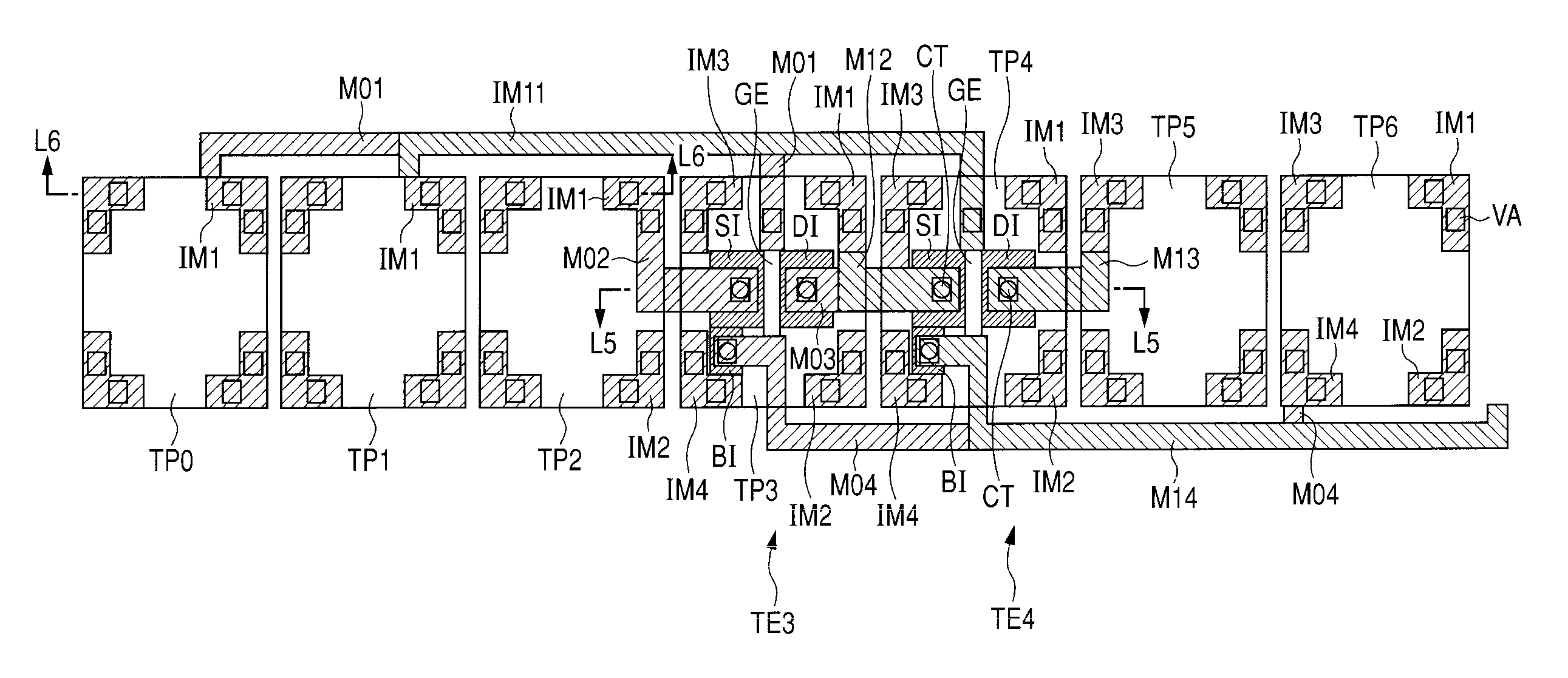
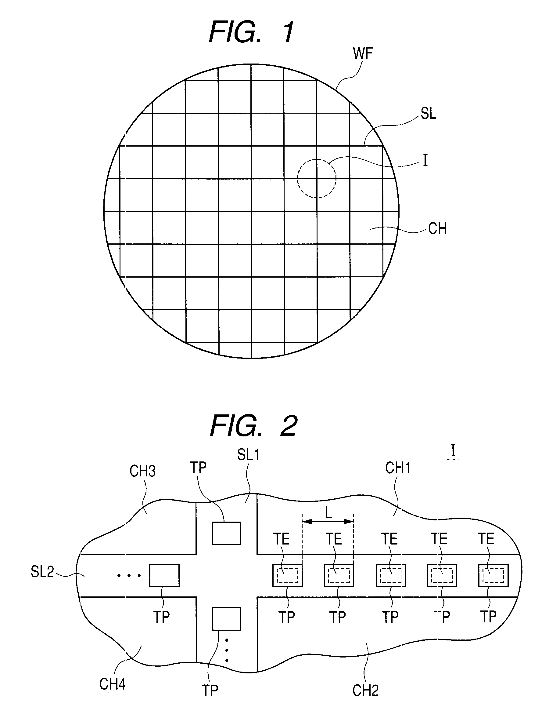
[0062]FIG. 1 is a diagram schematically showing a chip layout of a semiconductor wafer WF according to a first preferred embodiment of the present invention. In FIG. 1, a plurality of semiconductor chips CH are arranged over the semiconductor wafer WF in array form. Target semiconductor circuit devices are formed over these semiconductor chips CH. Scribe lines SL are formed to separate these semiconductor chips CH individually and mount or implement them in a package. After a wafer test process has been completed, the semiconductor chips CH formed over the semiconductor wafer WF are individually separated from one another by performing their dicing along the scribe lines SL. As will be described in detail later, test elements and test electrode pads that configure each TEG are placed in alignment in a signal row within areas with the scribe lines SL formed therein.

[0063]FIG. 2 is a diagram showing, in enlarged form, a broken-line area I lying over the semiconductor wafer WF shown in...

second preferred embodiment

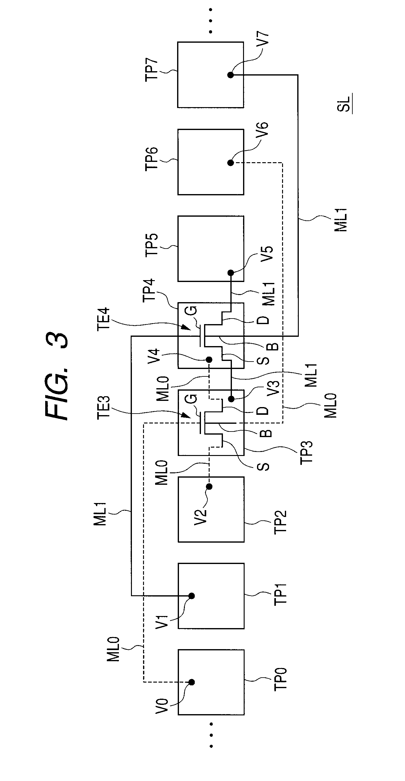
[0124]FIG. 14 is a diagram schematically showing a plan layout of a TEG according to a second preferred embodiment of the present invention. In FIG. 14, test electrode pads TPa through TPd are disposed in alignment in one row. Resistive elements R1 and R2 are formed in their corresponding areas lying directly below the test electrode pads TPb and TPc as test elements TE. The resistive element R1 is comprised of a first-layer metal wiring and the resistive element R2 is comprised of a second-layer metal wiring. The resistive element R1 is electrically coupled to the test electrode pads TPa and TPc adjacent thereto, and the resistive element R2 is electrically coupled to the test electrode pads TPb and TPd adjacent thereto. In a manner similar to the first preferred embodiment even in the configuration of the TEG shown in FIG. 14, island-like metal portions are provided corresponding to the test electrode pads for electrical couplings between the test electrode pads and the test eleme...

third preferred embodiment

[0150]FIG. 24 is a diagram schematically showing a plan layout of a TEG according to a third preferred embodiment of the present invention. In FIG. 24, test electrode pads TPa through TPd are placed in alignment in a single row in a manner similar to the second preferred embodiment. Capacitive elements CP1 and CP2 are respectively placed in areas lying directly below the test electrode pads TPb and TPc as a TEG. The capacitive element CP1 has electrode wirings PL1 and PL2 having comb's tooth portions. These comb's tooth portions are disposed so as to engage with each other. The electrode wirings PL1 and PL2 are respectively configured of a first-layer metal wiring and electrically coupled to the test electrode pads TPa and TPc.

[0151]The capacitive element CP2 has electrode wirings PL3 and PL4 each formed of a second layer wiring and has comb's tooth portions disposed opposite to each other in a manner similar to the above capacitive element.

[0152]These capacitive elements CP1 and CP...


PUM

PropertyMeasurementUnit
electrically couplingaaaaaaaaaa
areasaaaaaaaaaa
electricallyaaaaaaaaaa

Abstract

The present invention aims to increase the number of test elements of a TEG without increasing the area of each of slice areas. Test electrode pads are disposed in alignment in one row in each of areas separated from semiconductor chips provided over a semiconductor wafer. Test elements are formed corresponding to these test electrode pads and in areas lying directly therebelow. Electrode terminals of the test elements are electrically coupled to the test electrode pads adjacent to the corresponding electrode pads and the test electrode pads further adjacent thereto with being spaced one test electrode pad apart. Upon testing, probe pins are brought into contact with the odd-numbered test electrode pads to conduct testing. Next, the probe pins are brought into contact with the even-numbered test electrode pads while being shifted by one electrode pad pitch thereby to conduct testing.

Description

CROSS-REFERENCE TO RELATED APPLICATIONS[0001]The disclosure of Japanese Patent Application No. 2008-84460 filed on Mar. 27, 2008 including the specification, drawings and abstract is incorporated herein by reference in its entirety.BACKGROUND OF THE INVENTION[0002]The present invention relates to a configuration for efficiently laying out test elements for testing a semiconductor device at a semiconductor wafer level, and a test method using the test elements.[0003]A TEG (Test Element Group) is used to ensure the reliability of a semiconductor device such as an integrated circuit. The evaluation of a process, circuit characteristics and reliability is performed by a characteristic evaluation (test) using the TEG. At the stage of product development, a reliability evaluation is conducted based on the result of measurement using the TEG, and a process or circuit design is modified or corrected based on the so-obtained result of evaluation. As to actual products, the reliability of eac...

Claims


Application Information

Patent Timeline
Patent Type & Authority Applications(United States)
IPC IPC(8): G01R31/26H01L21/66H01L29/10G01R31/28
CPCG01R31/2831G01R31/2884H01L22/34Y10T29/49004H01L2924/0002H01L2924/00
Inventor SHINKAWATA, HIROKI
Owner RENESAS ELECTRONICS CORP
Why Eureka
Try Eureka