PCB layout structrue for suppressing EMI and method thereof

a layout structure and emi technology, applied in printed circuit aspects, high frequency circuit adaptations, magnetic/electric field screening, etc., can solve the problems of reducing the area of magnetic field on the pcb, reducing noise radiation, and increasing the noise of all electronic devices with high frequency signals

Inactive Publication Date: 2009-10-01
UNIVERSAL SCIENTIFIC INDUSTRIAL (SHANGHAI) CO LTD
View PDF5 Cites 22 Cited by
  • Summary
  • Abstract
  • Description
  • Claims
  • Application Information

AI Technical Summary

Benefits of technology

[0007]One particular aspect of the present invention is to provide a PCB layout structure for suppressing EMI and a method thereof that dispose a plurality of electric grids on the signal layer of the PCB to cover the signal lines on the si

Problems solved by technology

All electronic devices with high frequency signals will generate noise.
Generally, conducting interference is transmitted by the power wire and interferes with other electronic devices, and radiating interference is transmitted by radiation and interferes with other equipment.
As the technology has been developed, electroma

Method used


Image

  • PCB layout structrue for suppressing EMI and method thereof
  • PCB layout structrue for suppressing EMI and method thereof
  • PCB layout structrue for suppressing EMI and method thereof

Examples


Embodiment Construction

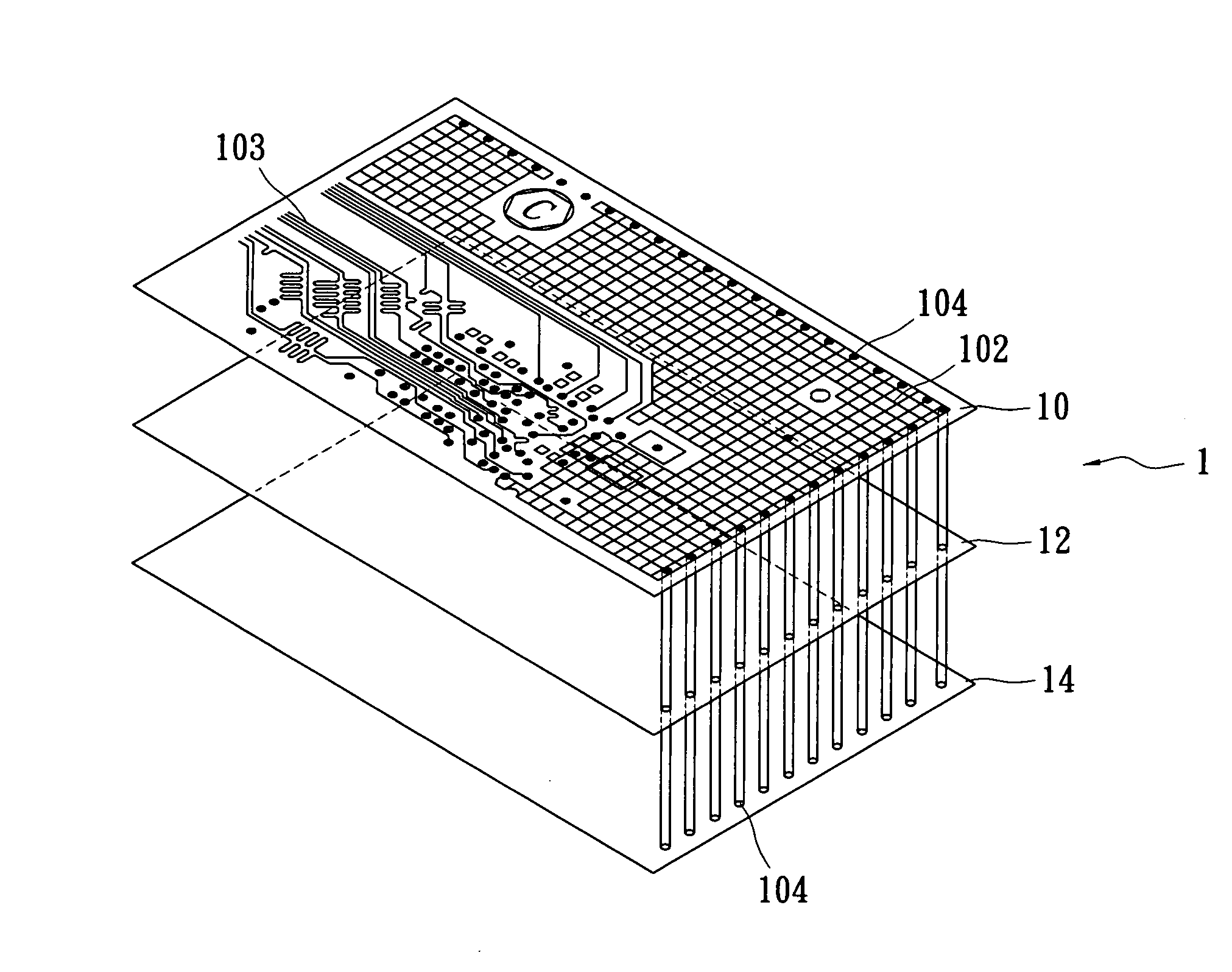
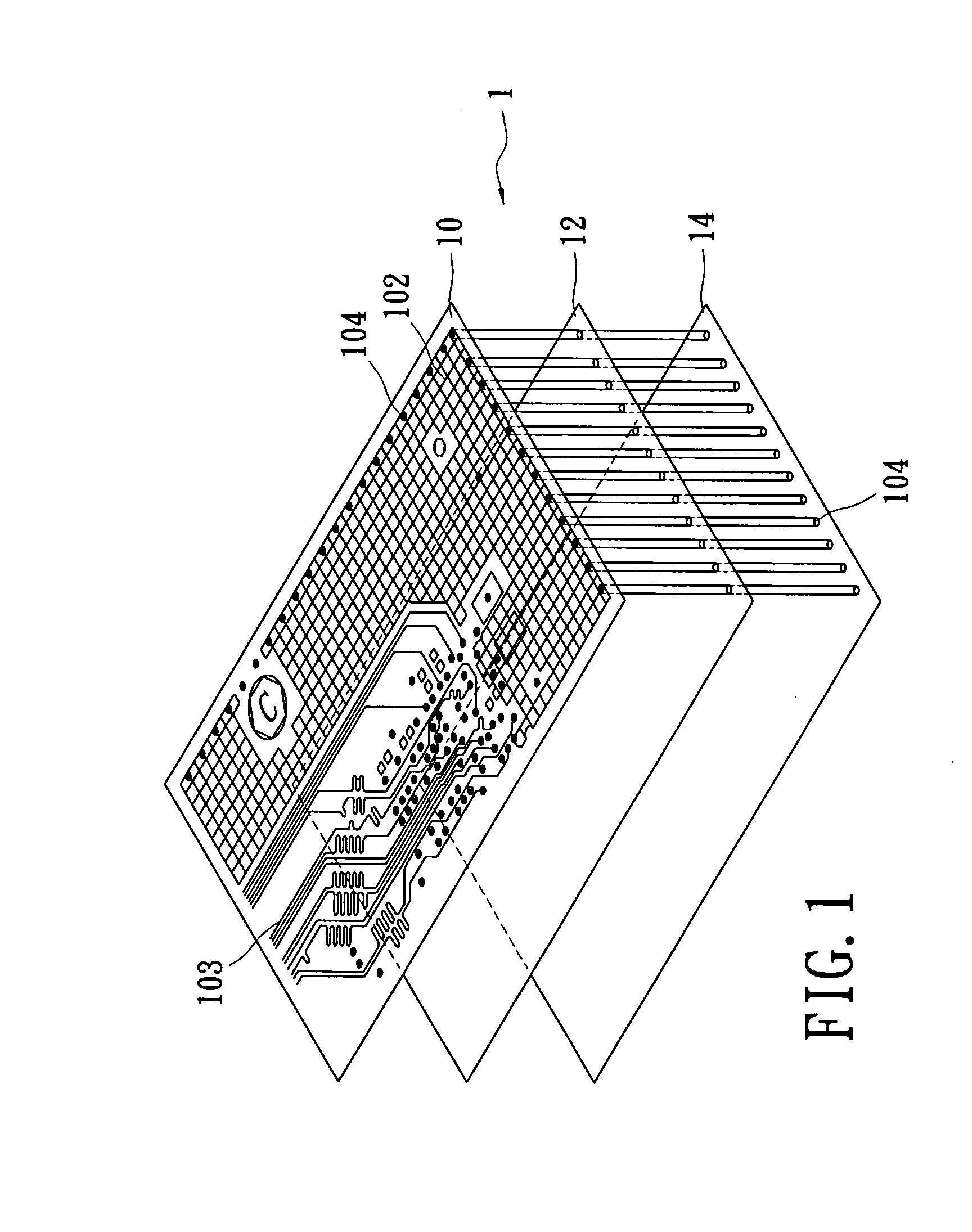
[0017]Reference is made to FIG. 1, which shows a schematic diagram of the PCB layout structure of the present invention. The PCB layout structure for suppressing EMI includes a multi-layer PCB 1, a plurality of electric grids 102, and a plurality of conductive vias 104. The multi-layer PCB 1 has a first signal layer 10, a second signal layer 14, and a grounding layer 12. The first signal layer 10 and the second signal layer 14 are disposed with a plurality of signal lines 103 and the plurality of electric grids 102. The electric grids 102 are used for covering the signal lines 103. The conductive vias 104 electrically connect the grounding layer 12 with the electric grids 102 on the first signal layer 10 and the second signal layer 14.

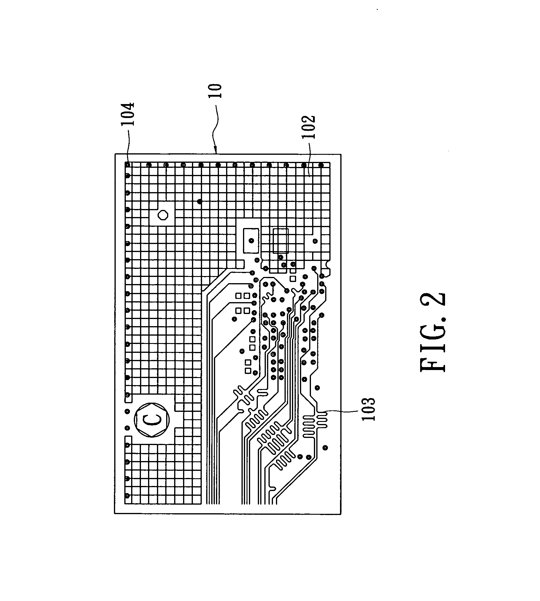
[0018]Reference is made to FIGS. 1 and 2. FIG. 2 shows a schematic diagram of the surface layer of the PCB of the present invention. A plurality of signal lines 103 are disposed on the first signal layer 10, and the signal lines 103 generate electromag...


PUM


Abstract

A PCB layout structure for suppressing EMI and a method thereof is disclosed. The PCB layout structure for suppressing EMI includes a multi-layer PCB, a plurality of electric grids, and a plurality of conductive vias. The multi-layer PCB has a plurality of signal layers and a grounding layer. Each of the signal layers is disposed with a plurality of signal lines. The plurality of electric grids are disposed on each of the signal layers and cover the signal lines on each of the signal layers. The plurality of conductive vias are located between the layers of the multi-layer PCB to electrically connect the grounding layer with the electric grids on each of the signal layers. Thereby, electromagnetic waves of a specific wavelength are shielded by appropriately choosing the dimensions of the electric grids.

Description

BACKGROUND OF THE INVENTION[0001]1. Field of the Invention[0002]The present invention relates to a PCB layout structure for suppressing EMI and a method thereof. In particular, this invention relates to a PCB layout structure and a method thereof that has high frequency signals and can suppress EMI.[0003]2. Description of the Related Art[0004]All electronic devices with high frequency signals will generate noise. Electronic noise can be divided into conducting interference and radiating interference. Generally, conducting interference is transmitted by the power wire and interferes with other electronic devices, and radiating interference is transmitted by radiation and interferes with other equipment. Therefore, the national electric equipment safety specification has a rule for regulating the EMI.[0005]As the technology has been developed, electromagnetic interference (EMI) becomes a key issue. When the speed of a semiconductor becomes faster and its density becomes heavy, noise a...

Claims


Application Information

Patent Timeline
IPC IPC(8): H05K9/00
CPCH05K1/0224H05K1/0225H05K1/0253H05K2201/09681H05K2201/09336H05K2201/09618H05K1/0298
Inventor YEH, WEI-HAOHUNG, YING-FU
Owner UNIVERSAL SCIENTIFIC INDUSTRIAL (SHANGHAI) CO LTD
Why Eureka
Try Eureka