Nitride-based semiconductor laser device and method of manufacturing the same

a laser device and semiconductor technology, applied in semiconductor lasers, lasers, active medium materials, etc., can solve the problems of kinks, asymmetric far-field patterns, disadvantageous instability of horizontal transverse modes, etc., and achieve excellent flatness, excellent flatness, excellent flatness

Inactive Publication Date: 2009-10-01
SANYO ELECTRIC CO LTD
View PDF4 Cites 10 Cited by
  • Summary
  • Abstract
  • Description
  • Claims
  • Application Information

AI Technical Summary

Benefits of technology

[0025]In this method of manufacturing a nitride-based semiconductor laser device according to the second aspect, as hereinabove described, the nitride-based semiconductor layer is formed on the main surface of the substrate formed with the recess portions, whereby when growing the nitride-based semiconductor layer, the first side surface formed by the (000-1) plane, having excellent flatness, can be formed starting from one of the recess portions in the two recess portions adjacent to each other, and the second side surface having excellent flatness can be formed starting from the other recess portion in the two recess portions adjacent to each other. The ridge having the optical waveguide is formed by the region held between these first and second side surfaces having excellent flatness, whereby the nitride-based semiconductor laser device having the optical waveguide, side surfaces of which have excellent flatness, can be obtained dissimilarly to a case of forming the optical waveguide by dry etching. Thus, the nitride-based semiconductor laser device having a stable horizontal transverse mode can be obtained.
[0026]The aforementioned method of manufacturing a nitride-based semiconductor laser device according to the second aspect preferably further comprises a step of separating into chips by dividing the nitride-based semiconductor layer into individual semiconductor laser devices on a region where the first side surface and the second side surface are opposed to each other, wherein the step of separating into chips includes a step of separating into chips by dividing the substrate into the individual semiconductor laser devices on bottom portions of the recess portions of the region where the first side surface and the second side surface are opposed to each other. According to this structure, a thickness of the substrate on the bottom portions of the recess portions is smaller than a thickness of the substrate on portions other than the bottom portions of the recess portions, and hence the device in a wafer state can be easily divided on portions of the substrate having a smaller thickness.
[0027]In the aforementioned method of manufacturing a nitride-based semiconductor laser device according to the second aspect, the step of growing the nitride-based semiconductor layer preferably includes a step of growing the nitride-based semiconductor layer so that the plane area of the nitride-based semiconductor layer is reduced in a direction away from the substrate along a thickness direction of the nitride-based semiconductor layer by inclining at least one of the first side surface and the second side surface with respect to the main surface of the substrate. According to this structure, the region (where the first side surface and the second side surface are opposed to each other in a wafer state) larger than the plane area of each recess portion of the substrate is formed on the surface of the semiconductor layer opposite to the substrate by the first side surface and the second side surface, and hence the wafer can be easily divided between the first side surface and the second side surface when separating the laser device into chips.
[0028]In the aforementioned method of manufacturing a nitride-based semiconductor laser device according to the second aspect, the substrate preferably includes a base substrate and an underlayer formed on the base substrate, and the step of forming the recess portions preferably includes a step of forming the recess portions on the underlayer. According to this structure, the nitride-based semiconductor layer having the first side surface formed by the (000-1) plane can be easily so formed as to start from the inner side surfaces of the recess portions by utilizing the recess portions formed on the underlayer when the nitride-based semiconductor layer is formed on the main surface of the base substrate.
[0029]In this case, the underlayer preferably includes an AlGaN layer, c1 and c2 preferably satisfy relation of c1>c2 when lattice constants of the base substrate and the underlayer are c1 and c2 respectively, and the step of forming the recess portions preferably includes a step of forming the recess portions formed by one of planes of a crack formed substantially parallel to a (0001) plane on the underlayer. According to this structure, when forming the underlayer made of AlGaN on the base substrate, the lattice constant c2 of the underlayer is smaller than the lattice constant c1 of the base substrate (c1>c2), and hence tensile stress is caused inside the underlayer in response to the lattice constant c1 of the base substrate. Consequently, the underlayer can not withstand this tensile stress, and hence the crack is formed on the underlayer along the (000-1) plane when the thickness of the underlayer is at least a prescribed thickness. Thus, a facet formed by (000-1) plane which is the basis for forming the (000-1) plane of the nitride-based semiconductor layer on the underlayer can be easily formed on the underlayer. Consequently, the nitride-based semiconductor layer having the first side surface formed by the (000-1) plane can be easily formed to start from the (000-1) facet formed by one of the planes of the crack formed on the underlayer when forming the nitride-based semiconductor layer on the substrate.

Problems solved by technology

L187-L189, however, the side walls of the ridge are not sufficiently flattened.
When the side walls of the ridge are not sufficiently flattened, a horizontal transverse mode is disadvantageously unstable.
When the horizontal transverse mode is unstable, a far-field pattern (FFP) is likely to be asymmetric and kink (nonlinearity) in I-L characteristics disadvantageously occurs.

Method used


Image

  • Nitride-based semiconductor laser device and method of manufacturing the same
  • Nitride-based semiconductor laser device and method of manufacturing the same
  • Nitride-based semiconductor laser device and method of manufacturing the same

Examples


first embodiment

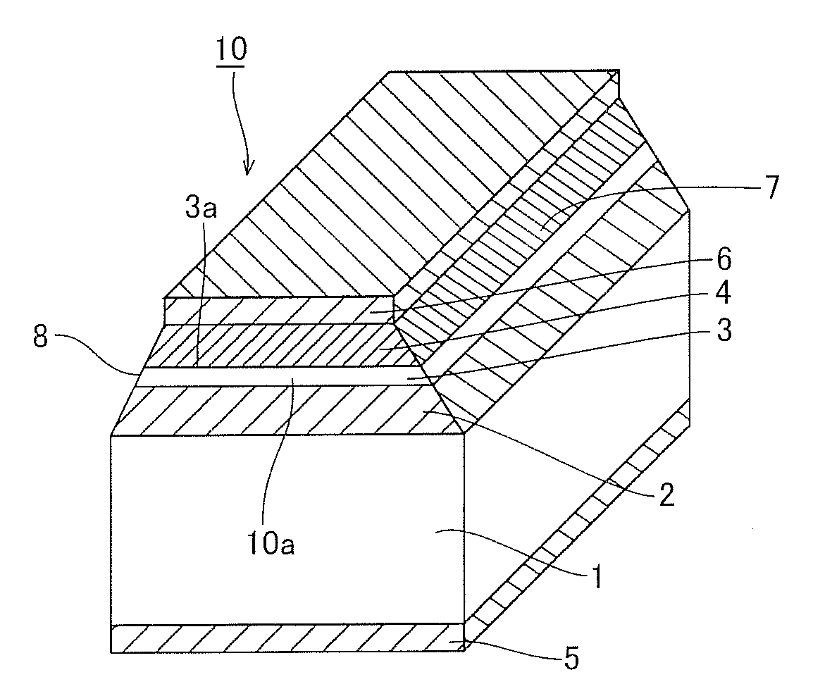
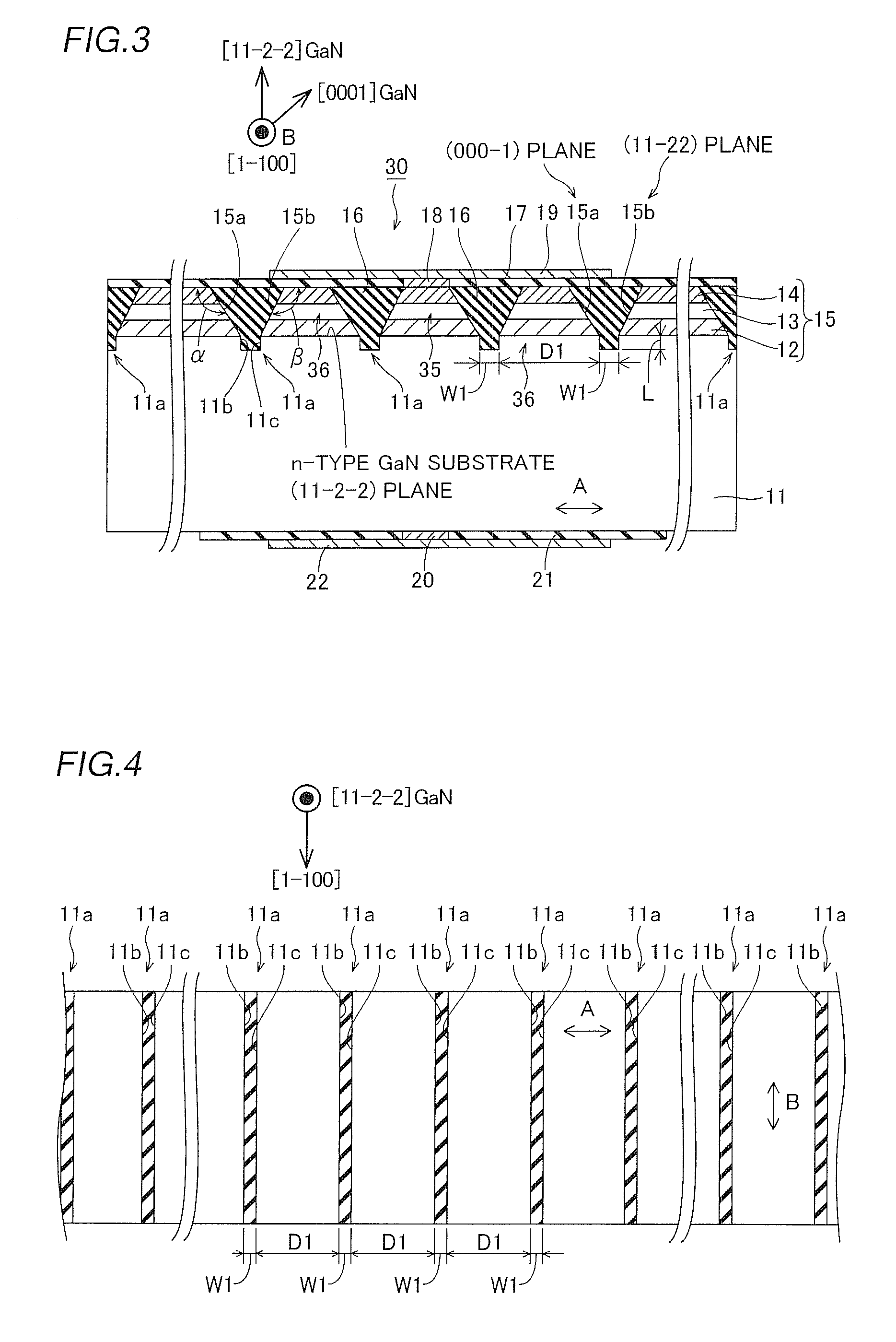
[0069]A structure of a nitride-based semiconductor laser device 30 according to a first embodiment will be now described with reference to FIG. 3.

[0070]This nitride-based semiconductor laser device 30 according to the first embodiment is formed by employing a wurtzite nitride semiconductor having a main surface formed by a (11-2-2) plane. As shown in FIG. 3, a light-emitting device layer 15 including an n-type cladding layer 12, an emission layer 13, a p-type cladding layer 14 is formed on an n-type GaN substrate 11 having a thickness of about 100 μm. The n-type cladding layer 12 is made of n-type Al0.05Ga0.95N, having a thickness of about 2.2 μm. The emission layer 13 has an MQW structure in which a well layer (not shown) made of Ga0.7In0.3N having a thickness of about 3 nm and a barrier layer (not shown) made of GaN having a thickness of about 20 nm are stacked. The p-type cladding layer 14 is made of p-type Al0.05Ga0.95N having a thickness of about 0.5 μm. The n-type GaN substrat...

second embodiment

[0089]According to a second embodiment, a light-emitting device layer 15 is formed after forming an underlayer 41 on an n-type GaN substrate 11 dissimilarly to the aforementioned first embodiment, which will be hereinafter described with reference to FIG. 7.

[0090]In a nitride-based semiconductor laser device 40 according to the second embodiment, the underlayer 41 made of Al0.05Ga0.95N having a thickness of about 3 to 4 μm is formed on the n-type GaN substrate 11. On this underlayer 41, a plurality of groove-shaped cracks 41a are so formed as to extend in a direction B. The cracks 41a are examples of the “recess portion” in the present invention. The n-type GaN substrate 11 according to the second embodiment is an example of the “base substrate” in the present invention.

[0091]The light-emitting device layer 15 including an n-type cladding layer 12, an emission layer 13, a p-type cladding layer 14 is formed on the underlayer 41. According to the second embodiment, first and second si...

third embodiment

[0098]According to a third embodiment, scribing cracks 41e are formed on an underlayer 41 so that formation positions of cracks 41a are controlled dissimilarly to the aforementioned second embodiment, which will be hereinafter described with reference to FIG. 11.

[0099]A nitride-based semiconductor laser device 50 according to the third embodiment is formed by employing a wurtzite nitride semiconductor having a main surface formed by a (10-12) plane. According to the third embodiment, on the underlayer 41, a plurality of the groove-shaped cracks 41a are formed at an interval D2 to extend in a direction B. According to the third embodiment, first side surfaces 15c formed by a (000-1) plane of the light-emitting device layer 15 and second side surfaces 15d formed by a (10-11) plane of the light-emitting device layer 15 are formed on the light-emitting device layer 15 to extend in a [11-20] direction. The first and second side surfaces 15c and 15d are inclined to sides opposite to each ...


PUM


Abstract

A nitride-based semiconductor laser device includes a nitride-based semiconductor layer formed on a main surface of a substrate and having an emission layer, wherein the nitride-based semiconductor layer includes a first side surface formed by a (000-1) plane and a second side surface inclined with respect to the first side surface, and a ridge having an optical waveguide extending perpendicular to a [0001] direction in an in-plane direction of the main surface of the substrate is formed by a region held between the first side surface and the second side surface.

Description

CROSS-REFERENCE TO RELATED APPLICATIONS[0001]The priority application numbers JP2008-90124, Nitride-Based Semiconductor Laser Device and Method of Manufacturing the Same, Mar. 31, 2008, Yasuto Miyake et al, JP2009-67213, Nitride-Based Semiconductor Laser Device and Method of Manufacturing the Same, Mar. 19, 2009, Yasuto Miyake et al, upon which this patent application is based are hereby incorporated by reference.BACKGROUND OF THE INVENTION[0002]1. Field of the Invention[0003]The present invention relates to a nitride-based semiconductor laser device and a method of manufacturing the same, and more particularly, it relates to a nitride-based semiconductor laser device provided with an optical waveguide and a method of manufacturing the same.[0004]2. Description of the Background Art[0005]In general, a light-emitting device made of a nitride-based material such as gallium nitride (GaN) has been put into practice as a 405 nm blue-violet semiconductor laser (LD) as a light source for r...

Claims


Application Information

Patent Timeline
Patent Type & Authority Applications(United States)
IPC IPC(8): H01S5/323H01L21/18H01L21/50
CPCB82Y20/00H01S5/0202H01S5/0207H01S5/028H01S5/0282H01S2301/185H01S5/22H01S5/2201H01S5/2214H01S5/34333H01S5/4031H01S5/2077
Inventor MIYAKE, YASUTOHIROYAMA, RYOJIHATA, MASAYUKIKUNO, YASUMITSU
Owner SANYO ELECTRIC CO LTD
Why Eureka
Try Eureka