Socket contact terminal and semiconductor device

a socket contact terminal and socket technology, applied in the direction of fixed connections, coupling device connections, manufacturing tools, etc., can solve the problems of high contact resistance, increased possibility of heat generation or voltage drop in response to higher current consumption, and difficulty in increasing the stroke, etc., to achieve high electrical connection, low resistance, and large current

Inactive Publication Date: 2009-10-08
THE FUJIKURA CABLE WORKS LTD
View PDF28 Cites 6 Cited by
  • Summary
  • Abstract
  • Description
  • Claims
  • Application Information

AI Technical Summary

Benefits of technology

[0122]Furthermore, since the terminal insertion hole is designed to have such a hole dimension that a gap is formed in at least a portion of a region between an inner wall of the terminal insertion hole and the contact terminal in a state where the contact terminal is inserted thereto, the elastomeric member expanded by being compressed upon application of a load to the contact terminal is received in the gap. Therefore, it is possible to prevent the housing and the elastomeric member from making frictional contact with each other, and thus, the contact terminal can maintain preset load-displacement characteristics.
[0123]Furthermore, by providing a beam part to the contact terminal so that the beam part is press-fitted to an engagement portion of the housing, it is possible to prevent the elastomeric member from making contact with the housing. Therefore, even when the contact terminal has been engaged with the housing, it is possible to maintain the load-displacement characteristics of a single body of the contact terminal.
[0124]Furthermore, since the housing is formed of an elastomeric member, even when a substrate has some degree of warpage, the housing might assume the warped shape of the substrate so that the substrate and the socket can be in close contact with each other, and it is thus possible to secure a high electrical connection.
[0125]Furthermore, since the semiconductor device according to this aspect of the invention includes the socket according to the above aspect of the invention, a printed circuit board, and an IC package, the printed circuit board and the IC package being electrically connected with each other through the intervention of the socket, it is possible to provide a high-performance device or apparatus capable of providing low resistance, large current and fast operation speed requirements.

Problems solved by technology

Therefore, there is a problem that it is difficult to increase the stroke when the pins are made to have a finer pitch.
However, when the conductive elastomeric member as disclosed in Patent Document 3 is used, since the contact terminal is not a metal but an elastomeric member, the contact resistance is high compared with a metallic contact and there is a fear of an increasing possibility of heat generation or voltage drop in response to higher current consumption.
Moreover, since the contact terminal does not wipe a metallic land when it is inserted to be fitted in a package, there occurs a new problem that it is difficult to remove an oxide film formed on a land.

Method used


Image

  • Socket contact terminal and semiconductor device
  • Socket contact terminal and semiconductor device
  • Socket contact terminal and semiconductor device

Examples


embodiment 1

[0259]A description of an embodiment of the present invention will be provided with reference to the drawings.

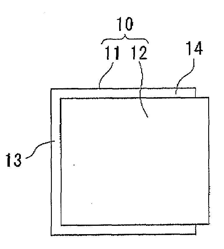
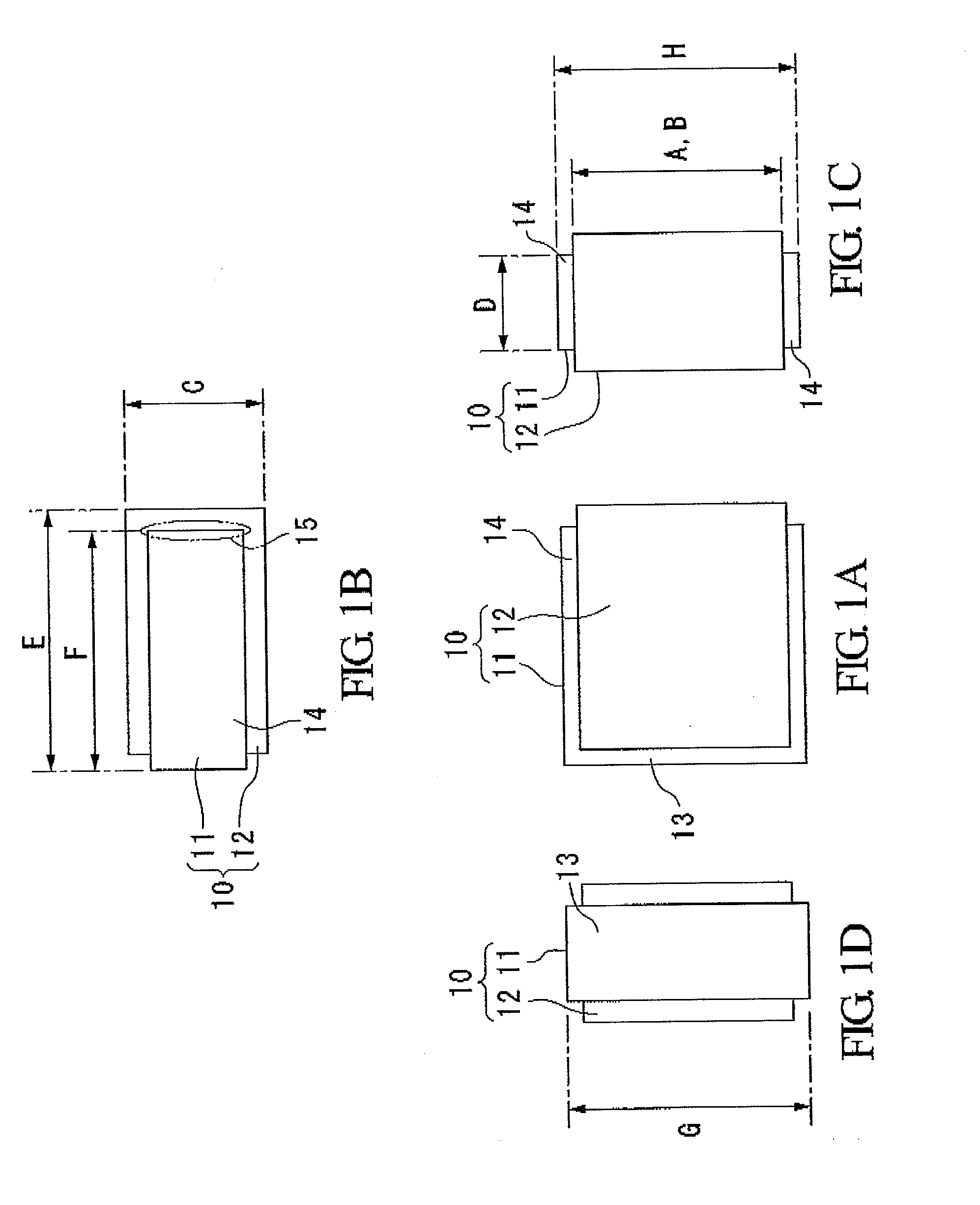
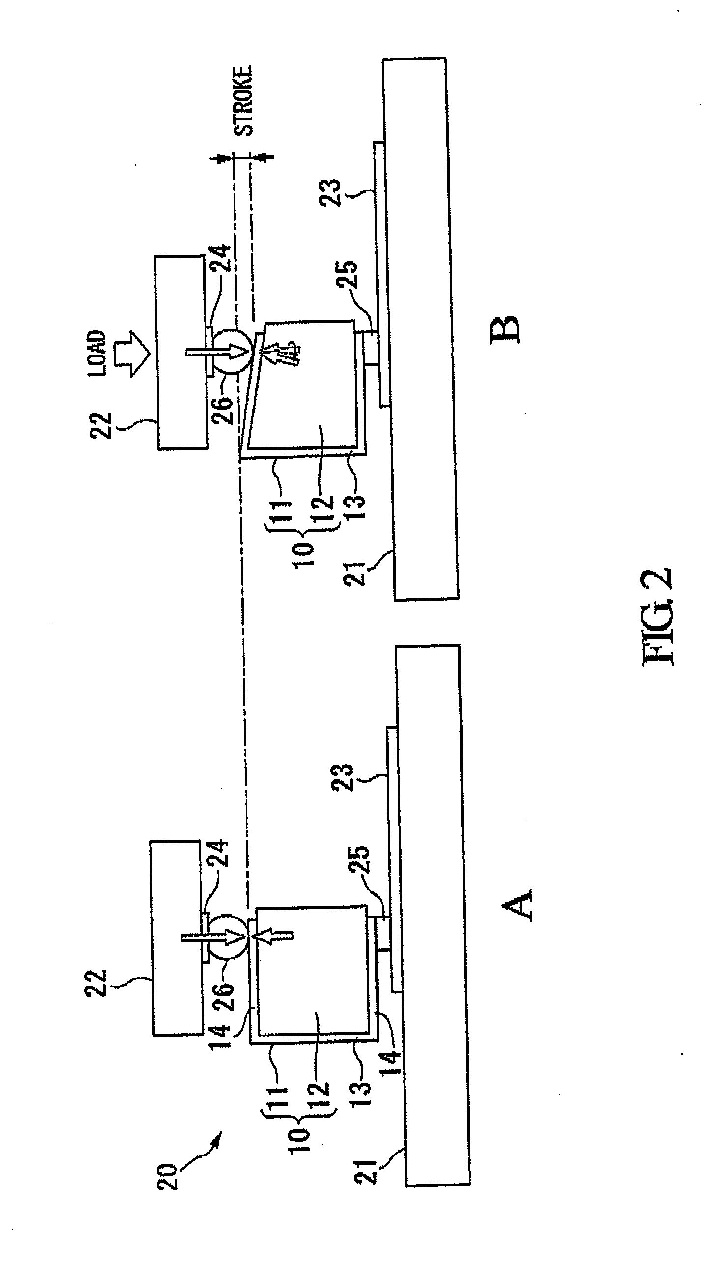
[0260]FIGS. 1A to 1D are views illustrating a socket contact terminal (hereinafter referred to simply as a contact terminal) according to a first embodiment of the present invention, in which FIG. 1A is a side view of the contact terminal 10, FIG. 1B is a top plan view thereof, FIG. 1C is a front view thereof, and FIG. 1D is a rear view thereof. In the drawing figures, reference numeral 10 designates a contact terminal, 11 designates a metal terminal, 12 designates an elastomeric member, 13 designates a main columnar portion, 14 designates an arm portion, and 15 designates a contact portion.

[0261]The contact terminal 10 according to the present embodiment is configured to provide electrical connection between a connection portion formed of a metal conductor on a printed circuit board and a connection terminal of an IC package and includes a metal terminal 11 having an angula...

embodiment 2

[0274]FIGS. 3A to 3D are views illustrating a contact terminal according to a second embodiment of the present invention. In FIG. 3, only a metal terminal 31 of the contact terminal 30 according to the present embodiment is illustrated. FIG. 3A is a top plan view of the metal terminal 31, FIG. 3B is a side view thereof, and FIG. 3C is a rear view thereof. In the drawings, reference numeral 31 designates a metal terminal, 32 designates a main columnar portion, 33 designates an arm portion, 34 designates a wide and thick portion, and 35 designates a dome-shaped convex portion.

[0275]The contact terminal 30 according to the present embodiment includes substantially the same components as those of the contact terminal 10 according to the first embodiment described above, and is characterized in that a dome-shaped convex portion 35 is provided on an outer surface of each of the arm portions 33 of the metal terminal 31, and that a wide and thick portion 34 is provided on a central portion ...

embodiment 3

[0284]FIG. 4 is a view illustrating a contact terminal according to a third embodiment of the present invention. In FIG. 4, only a metal terminal 41 of the contact terminal according to the present embodiment is illustrated. FIG. 4A is a side view of the metal terminal 41, FIG. 4B is a top plan view thereof, and FIG. 4C is a rear view thereof. In the drawing, reference numeral 41 designates a metal terminal, 42 designates a main columnar portion, 43 designates an arm portion, 44 designates a wide and thick portion, and 45 designates a semi-cylindrical convex portion.

[0285]The contact terminal according to the present embodiment includes substantially the same components as those of the contact terminal 30 according to the second embodiment described above, and is characterized in that a semi-cylindrical convex portion 45 is provided on each of the arm portions 43 of the metal terminal 41 by means of bending. Moreover, similar to the contact terminal 30 according to the second embodi...


PUM

PropertyMeasurementUnit
displacementaaaaaaaaaa
frequencyaaaaaaaaaa

Abstract

A socket contact terminal for electrical connection between a connection portion formed of a metal conductor on a printed circuit board and a connection terminal of an IC package. The contact terminal comprises a metal terminal composed of a main columnar portion and arm portions on both sides and having an angular U shape and an elastomeric member attached to the metal terminal. A metal surface is exposed from the outer surface of each arm portion. The elastomeric member is firmly held between the arm portions of the metal terminal and exhibits a repulsive force when the arm portions are pressed in the direction that the arm portions approach each other.

Description

TECHNICAL FIELD[0001]The present invention relates to an IC socket contact terminal used for mounting an IC package such as a CPU or an LSI on a printed circuit board. More particularly, the present invention relates to a socket contact terminal which can be suitably used for mounting an IC package such as an LGA package or a BGA package on a printed circuit board, and to a semiconductor device using the same.[0002]This application is based upon and claims the benefit of priority from prior Japanese Patent Application Nos. 2006-149510 filed at the Japan Patent Office on May 30, 2006, 2006-154545 filed at the Japan Patent Office on Jun. 2, 2006, 2006-158670 filed at the Japan Patent Office on Jun. 7, 2006, 2006-162508 filed at the Japan Patent Office on Jun. 12, 2006, and 2006-162509 filed at the Japan Patent Office on Jun. 12, 2006, the contents of which are hereby incorporated by reference in their entirety.BACKGROUND ART[0003]Hitherto, there has been studied a technique for mounti...

Claims


Application Information

Patent Timeline
Patent Type & Authority Applications(United States)
IPC IPC(8): H01R33/76H01R13/40H01R43/20H05K1/16H01R12/55H01R12/58
CPCH01L2924/3511H01R13/2485Y10T29/53209H01R12/52H01R12/714H05K7/1069H01R12/55H01R12/58H01R33/76
Inventor OUCHI, YASUHIRONIKAIDO, SHINICHIMIYAZAWA, HARUOWATANABE, HIROHITOYAMAGAMI, KATSUYA
Owner THE FUJIKURA CABLE WORKS LTD
Why Eureka
Try Eureka