Dichalcogenide thermoelectric material

a thermoelectric material and dichalcogenide technology, applied in the direction of basic electric elements, metal selenides/tellurides, selenium/tellurium compounds with other elements, etc., can solve the problems of low thermal conductivity of the c-axis direction, many thermoelectric materials perform well, and achieve low thermal conductivity , large power factor

Inactive Publication Date: 2009-10-08
SAMSUNG ELECTRONICS CO LTD
View PDF12 Cites 22 Cited by
  • Summary
  • Abstract
  • Description
  • Claims
  • Application Information

AI Technical Summary

Benefits of technology

[0018]The present disclosure provides a dichalcogenide thermoelectric material having a very low

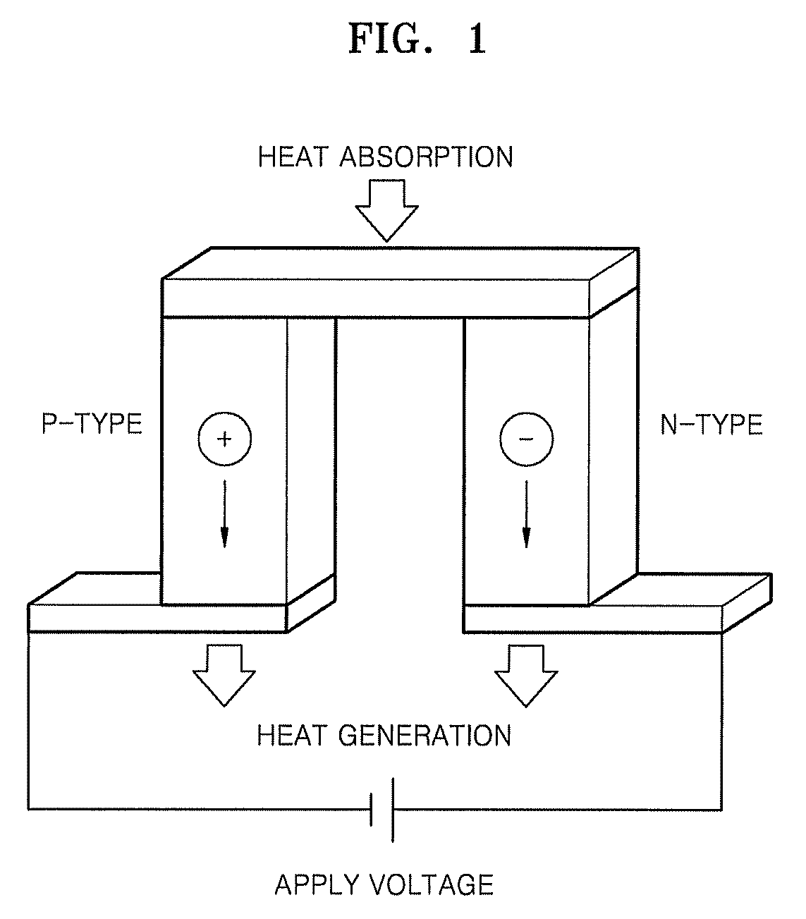
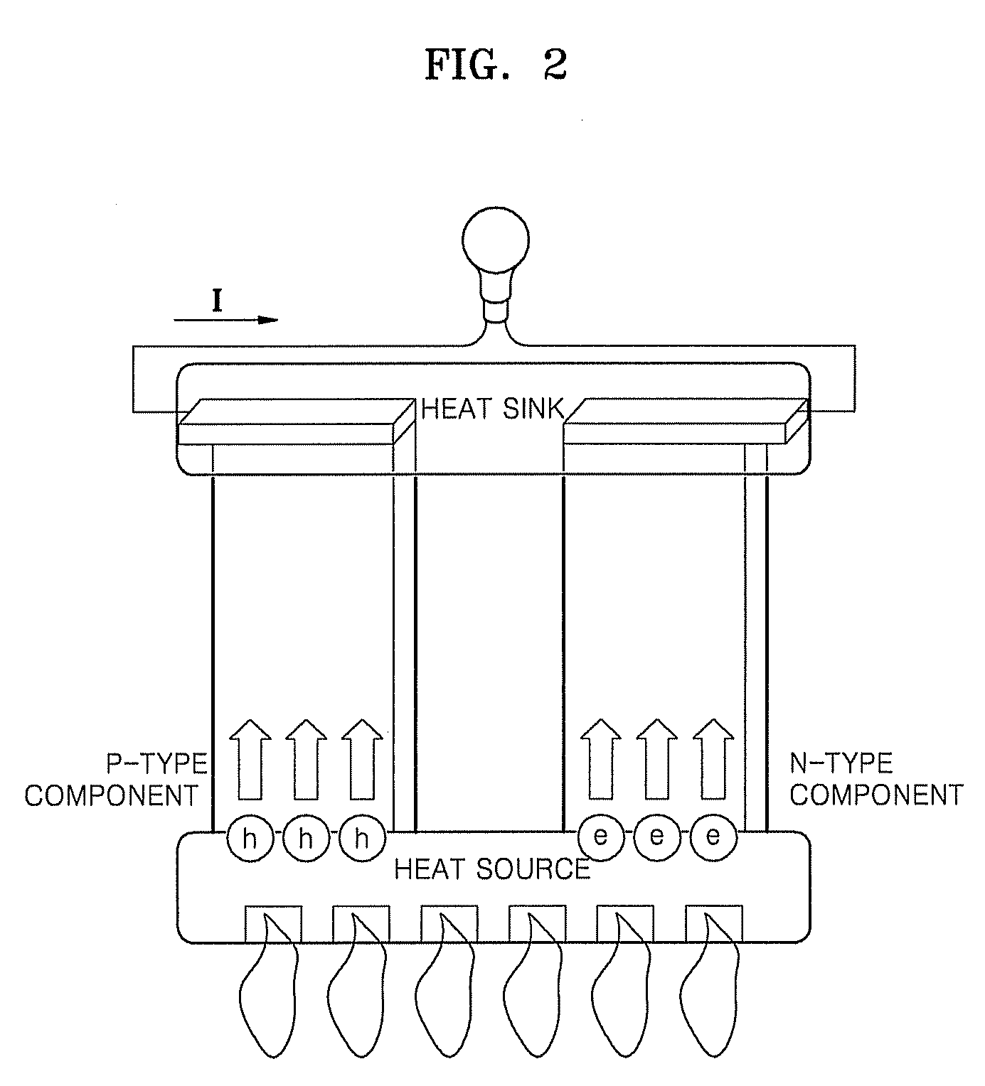
Problems solved by technology

However, many thermoelectric materials perform well only in a range of room temperature to high temperature.
Accordingly, the thermoelectric material disclosed in this application is not in wide use.
This means that materials having a 2-dimensional disordered and layered structure within the in-plane direction, but regularly stacked

Method used


Image

  • Dichalcogenide thermoelectric material
  • Dichalcogenide thermoelectric material
  • Dichalcogenide thermoelectric material

Examples


example 1

[0089]A polycrystalline thermoelectric material was synthesized by the ampoule method using an ampoule. First, Ce, Te, and Sn as material elements were quantified in a predetermined ratio and added to an ampoule made of a quartz tube. Then, the ampoule with the material element was sealed in a vacuum and heat treated at 850° C. for 24 hours to respectively synthesize rare earth dichalcogenide CeTe2, CeTe1.95Sn0.05, CeTe1.9Sn0.1, CeTe1.7Sn0.3, CeTe1.5Sn0.5, and CeTeSn. Mole ratios of CeTe2, CeTe1.95Sn0.05, CeTe1.9Sn0.1, CeTe1.7Sn0.3, CeTe1.5Sn0.5, and CeTeSn are checked by using an inductively coupled plasma spectroscopy.

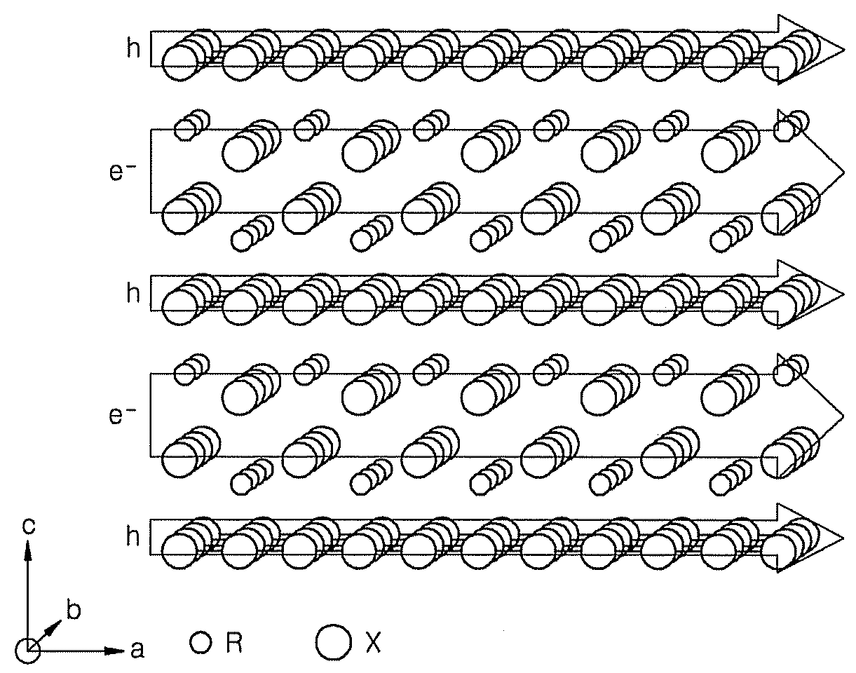
[0090]CeTe2 has a two-dimensional layered structure, and a weak ionic bond between a Te layer and a Ce—Te block is formed. CeTe2-xSnx has a structure in which Sn is doped to substitute a part of Te in CeTe2.

example 2

[0091]A polycrystalline thermoelectric material was synthesized by the ampoule method. First, Ce, Se, and Sn as material elements were quantified in a predetermined ratio and added to an ampoule made of a quartz tube. Then, the ampoule with the material element was sealed in a vacuum and heat treated at 850° C. for 24 hours to respectively synthesize rare earth dichalcogenide CeSe2, CeSe1.9Sn0.1, CeSe1.8Sn0.2, and CeSe1.5Sn0.5. Mole ratios of CeSe2, CeSe1.9Sn0.1, CeSe1.8Sn0.2, and CeSe1.5Sn0.5 are checked by using an inductively coupled plasma spectroscopy.

[0092]CeTe2 has a flat orthorhombic structure in a direction of b-axis as illustrated in FIG. 4, and has a two-dimensional layered structure, and a weak ionic bond between a Se layer and a Ce—Se block is formed. CeTe2-xSnx has a structure in which Sn is doped to substitute a part of Se in CeSe2.

experimental example 1

Measurement of Thermal Conductivity

[0093]Thermal conductivities of CeTe2, CeTe1.95Sn0.05, CeTe1.95Sn0.1, CeTe1.5Sn0.5, and CeTeSn prepared in Example 1 are illustrated in FIG. 5, and the thermal conductivities are measured by measuring thermal relaxation via a laser flash method. As illustrated in FIG. 5, CeTe2, CeTe1.95Sn0.05, CeTe1.95Sn0.1, CeTe1.5Sn0.5, and CeTeSn have very low thermal conductivities, and specifically, CeTe2 and CeTe1.95Sn0.05 have very low thermal conductivities in a range of about 1.50 to about 1.58 Wm−1K−1 at 300 K. In addition, the conductivity values of CeTe2 and CeTe1.95Sn0.05 are approximately 55% lower than commercially available Sb-doped Bi2Te3, and is significantly lower than other thermoelectric materials. When a mole ratio x of Sn in CeTe2-xSnx is equal to or above 1.0, thermal conductivity increases, and thus performance decreases. Thermal conductivities of CeTe2 and CeTe0.5Sn0.5 are compared with those of other commercially available thermoelectric ...


PUM

PropertyMeasurementUnit
Temperatureaaaaaaaaaa
Compositionaaaaaaaaaa
Structureaaaaaaaaaa

Abstract

A dichalcogenide thermoelectric material having a very low thermal conductivity in comparison with a conventional metal or semiconductor is described. The dichalcogenide thermoelectric material has a structure of Formula 1 below:
RX2-aYa  Formula 1
wherein R is a rare earth or transition metal magnetic element, X and Y are each independently an element selected from the group consisting of S, Se, Te, P, As, Sb, Bi, C, Si, Ge, Sn, B, Al, Ga, In, and a combination thereof, and 0≦a<2.

Description

CROSS-REFERENCE TO RELATED PATENT APPLICATION[0001]This application claims priority to Korean Patent Application No. 10-2008-0031709, filed on Apr. 4, 2008 and 10-2008-0070791, filed on Jul. 21, 2008, in the Korean Intellectual Property Office, and all the benefits accruing therefrom under 35 U.S.C. § 119, the contents of which are both hereby incorporated in their entirety by reference.BACKGROUND OF THE INVENTION[0002]1. Field of the Invention[0003]The present disclosure relates to a dichalcogenide thermoelectric material having a very low thermal conductivity in comparison with a conventional metal or semiconductor.[0004]2. Description of the Related Art[0005]In general, thermoelectric materials can be utilized in active cooling, waste heat power generation, and the like by using the Peltier effect and the Seebeck effect. FIG. 1 is a schematic diagram illustrating thermoelectric cooling using the Peltier effect. Referring to FIG. 1, the Peltier effect occurs when a DC voltage is a...

Claims


Application Information

Patent Timeline
IPC IPC(8): H01L35/16
CPCC01B17/20C01B19/002C01B19/007C01P2002/20H01L35/16C01P2002/77C01P2006/32C01P2006/40C01P2002/52H10N10/852
Inventor RHYEE, JONG-SOOLEE, SANG-MOCK
Owner SAMSUNG ELECTRONICS CO LTD
Why Eureka
Try Eureka