Method of processing a semiconductor substrate by thermal activation of light elements

a technology of light elements and semiconductors, applied in the direction of photovoltaic energy generation, crystal growth process, electrical equipment, etc., can solve the problems of significant degradation of the efficiency of the photovoltaic cells produced from this silicon, the efficiency of the photovoltaic cells such as this remains lower than the efficiency of the photovoltaic cells made with electronic-grade silicon substrates, and the excessive quantity of doping impurities. to achieve the effect of improving the electrical quality of the semiconductor

Inactive Publication Date: 2009-10-08
COMMISSARIAT A LENERGIE ATOMIQUE ET AUX ENERGIES ALTERNATIVES
View PDF8 Cites 17 Cited by
  • Summary
  • Abstract
  • Description
  • Claims
  • Application Information

AI Technical Summary

Benefits of technology

[0007]Thus there is a need to propose a method of processing a semiconductor-based substrate which, in particular when the substrate is semiconductor-based and comprises several types of light

Problems solved by technology

Although this extraction of metallic impurities partially purifies this type of silicon, the efficiency of a photovoltaic cell such as this remains lower than the efficiency of a photovoltaic cell made with an electronic-grade silicon substrate, because of the presence of high concentrations of doping impurities.
The energy conversion efficiency of photovoltaic cells manufactured from a semiconductor such as silicon that has been purified by metallurgical methods or by chemical degradation is therefore generally limited

Method used


Image

  • Method of processing a semiconductor substrate by thermal activation of light elements
  • Method of processing a semiconductor substrate by thermal activation of light elements
  • Method of processing a semiconductor substrate by thermal activation of light elements

Examples


Embodiment Construction

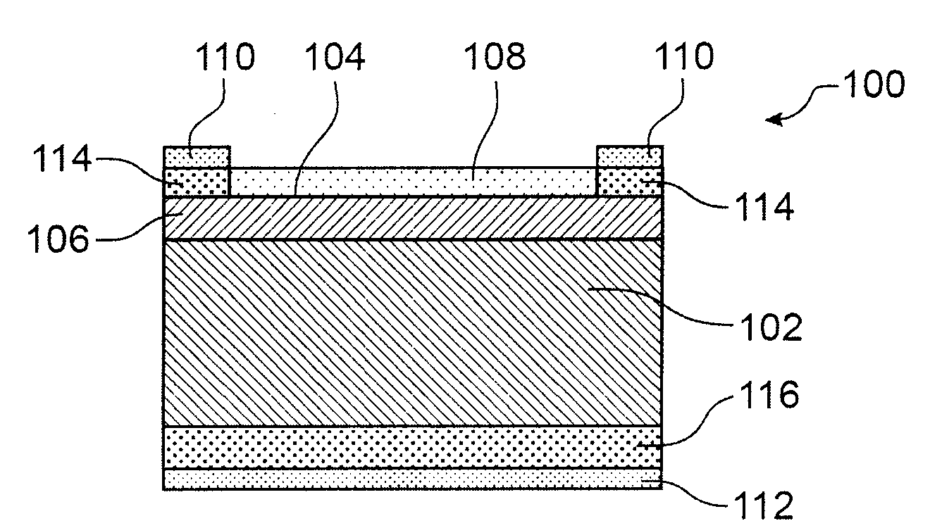
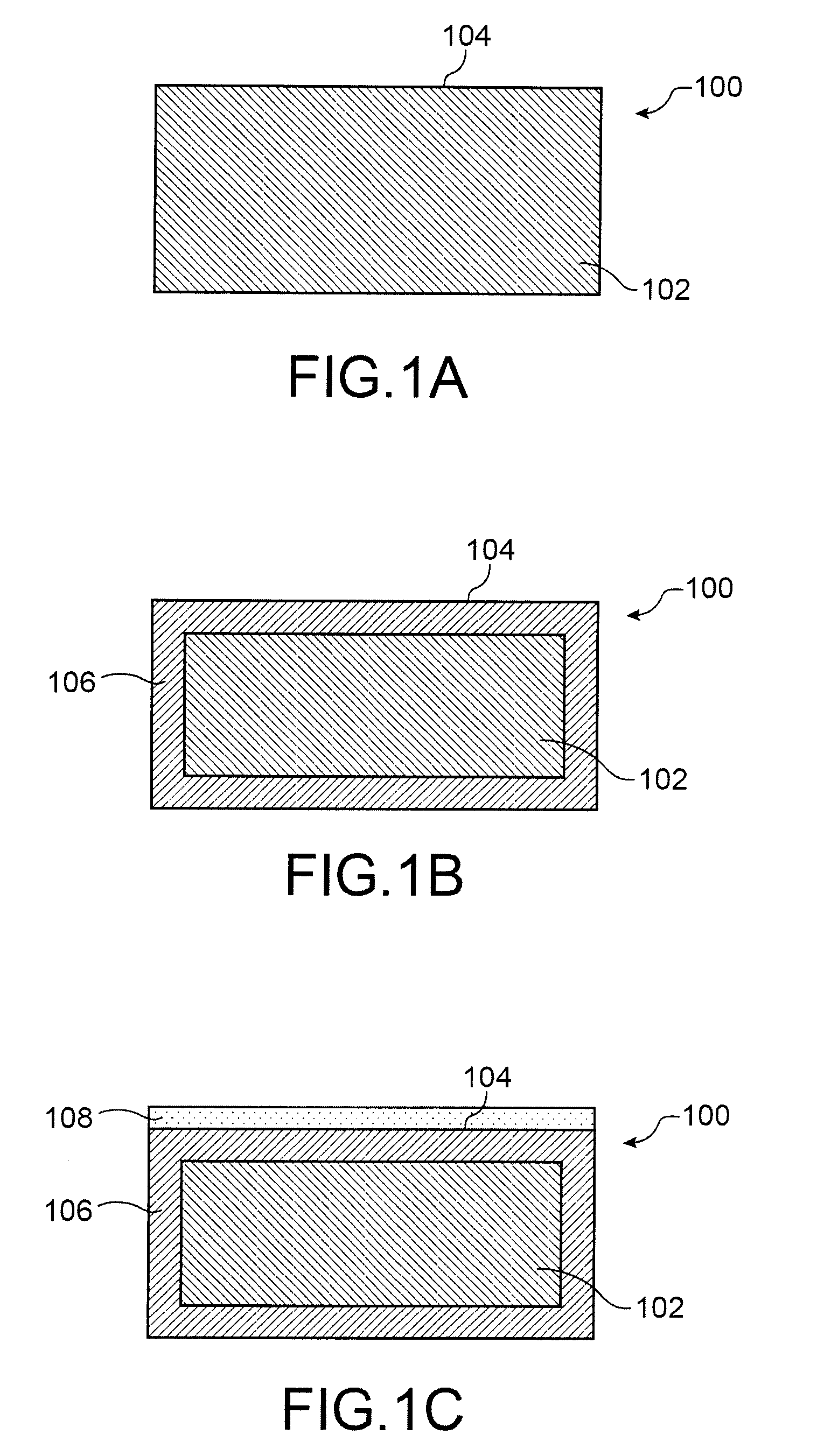
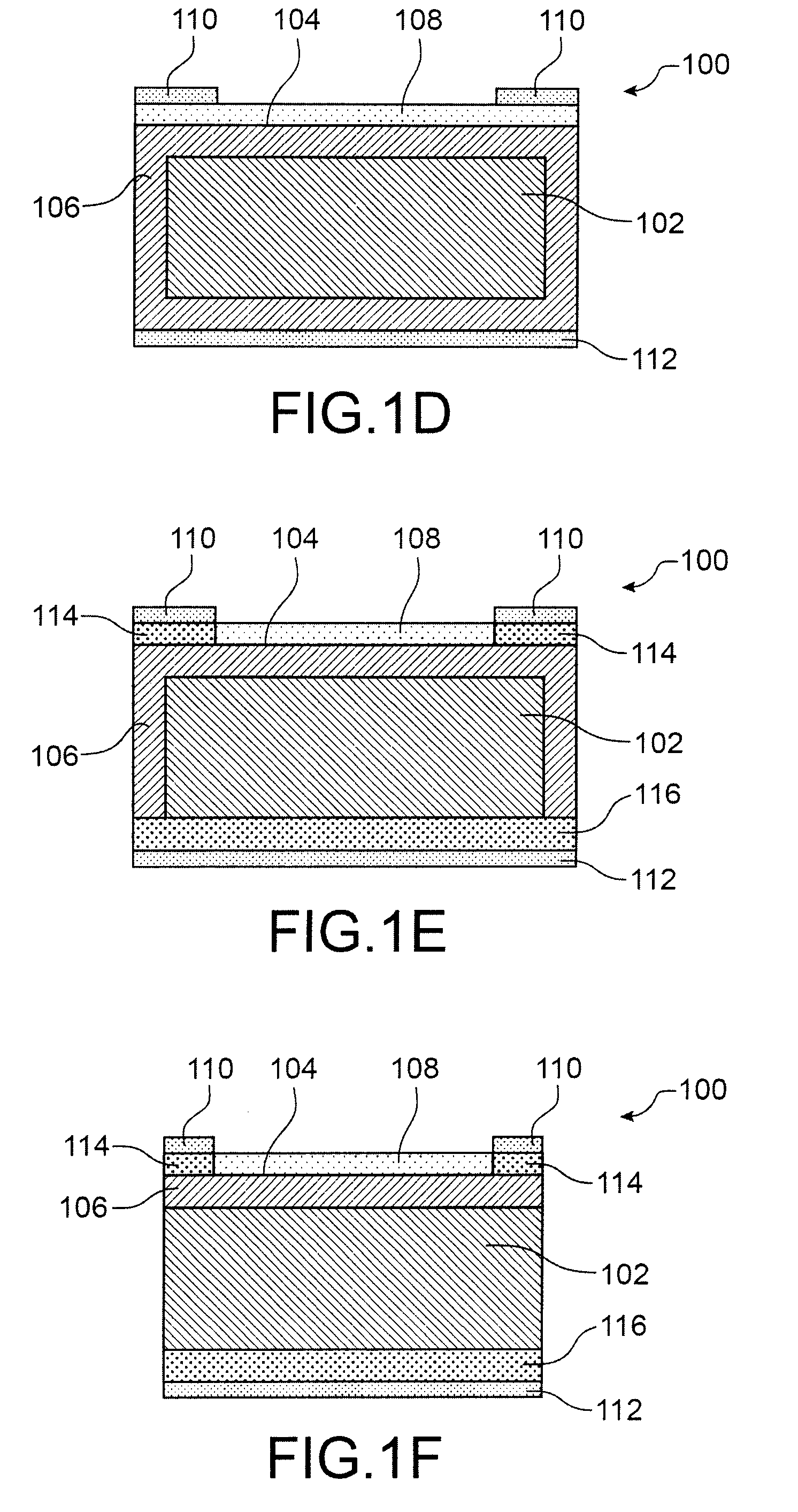
[0067]Reference is made first to FIGS. 1A to 1F, which show the steps of a method of producing a photovoltaic cell 100 according to a first exemplary embodiment.

[0068]As shown in FIG. 1A, the photovoltaic cell 100 is produced from a semiconductor-based substrate 102, e.g., p-type crystalline silicon. This silicon, e.g., monocrystalline and obtained by Cz growth, comprises significant concentrations of doping impurities, and born in particular. These concentrations, for example, may be between approximately 1015 cm−3 and 3.1018 cm−3. Furthermore, given that this silicon was obtained by Cz growth, it likewise comprises a significant quantity of light elements, particularly oxygen, which, for example, may be between approximately 1017 cm−3 and 5.1018 cm−3.

[0069]To produce the photovoltaic cell 100, a texturing of the face 104 of the substrate 102 is first carried out, this face 104 being intended to form the front face of the photovoltaic cell 100, i.e., the face intended to receive th...


PUM


Abstract

Method of processing a substrate containing at least one semiconductor of the SiXAY type and comprising at least four separate types of light elements, comprising at least the following steps:
    • carrying out a first anneal of the substrate at a temperature T1 corresponding to a thermal activation temperature for a first one of the four types of light elements,
    • carrying out a second anneal of the substrate at a temperature T2 corresponding to a thermal activation temperature for a second one of the four types of light elements,
    • carrying out a third anneal of the substrate at a temperature T3 corresponding to a thermal activation temperature for a third one of the four types of light elements,
    • carrying out a fourth anneal of the substrate at a temperature T4 corresponding to a thermal activation temperature for a fourth one of the four types of light elements,
    • each anneal comprising a holding at the temperature T1, T2, T3 or T4 and the temperatures T1, T2, T3 and T4 being such that T1>T2>T3>T4.

Description

TECHNICAL FIELD[0001]This invention relates to a method of processing a semiconductor-based substrate by thermal activation of light elements present in the substrate. The invention likewise relates to a method of producing a semiconductor device from a substrate comprising thermally activated light elements. The invention is particularly applicable to the production of photovoltaic cells.PRIOR ART[0002]A considerable amount of research relates to the production of crystalline silicon (monocrystalline or polycrystalline) for the production of substrates, in particular within the field of photovoltaic applications, from silicon that has been purified by metallurgical methods or by chemical degradation. The silicon obtained from these new sources generally contains concentrations of metallic impurities (e.g., iron, chromium, copper, etc.), doping impurities (e.g., boron, phosphorous, aluminium, etc.), and light elements (e.g., oxygen, nitrogen, carbon, hydrogen, etc.) which are much h...

Claims


Application Information

Patent Timeline
IPC IPC(8): H01L21/322H01L31/0232H01L31/0236
CPCC30B29/52C30B33/02H01L21/3225H01L21/3242Y02E10/546H01L31/1812H01L31/182H01L31/1864H01L31/03685Y02P70/50
Inventor DUBOIS, SEBASTIENENJALBERT, NICOLASMONNA, REMI
Owner COMMISSARIAT A LENERGIE ATOMIQUE ET AUX ENERGIES ALTERNATIVES
Why Eureka
Try Eureka