

Wireless IC device
a wireless ic device and wireless technology, applied in the direction of protective material radiating elements, near-field systems using receivers, instruments, etc., can solve the problems of increasing the cost of the tag, increasing the design complexity of the tag, increasing the number of design parameters, etc., to facilitate the design the effect of reducing the size and cost of the wireless ic devi
- Summary
- Abstract
- Description
- Claims
- Application Information
AI Technical Summary
Benefits of technology
Problems solved by technology
Method used
Image

Examples
first preferred embodiment
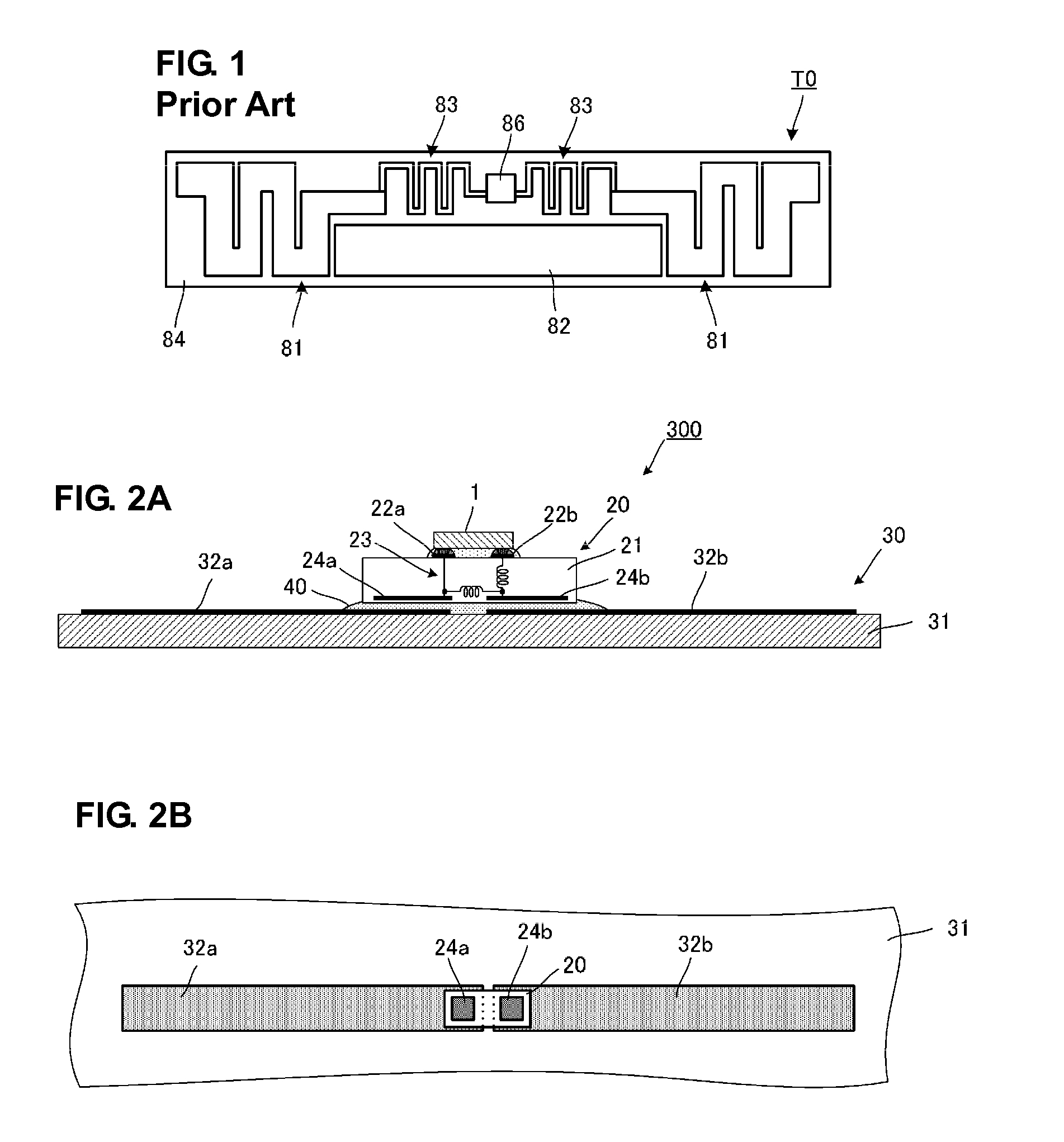
[0064]A wireless IC device according to the first preferred embodiment of the present invention will be described with reference to FIGS. 2A to 5. FIG. 2A is a cross-sectional view of a main portion of a wireless IC device according to the first preferred embodiment. FIG. 2B is a plan view of the main portion of the wireless IC device.
[0065]As illustrated in FIG. 2A, a wireless IC device 300 includes a wireless IC chip 1, a functional substrate 20, and a radiation plate 30. The wireless IC chip 1 is preferably a semiconductor chip including a signal processing circuit functioning as an RFID tag, for example.
[0066]The radiation plate 30 includes radiation electrodes 32a and 32b provided on the upper surface of a base material 31, such as a PET film, for example.
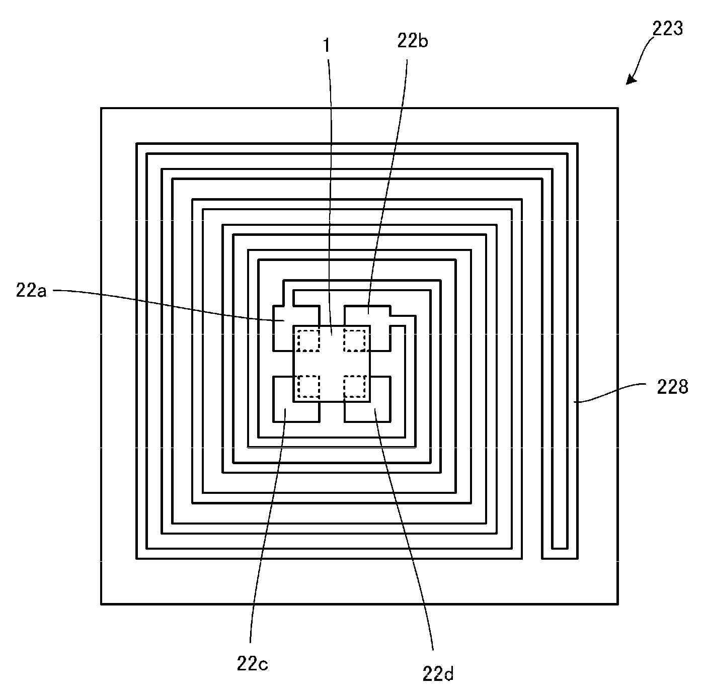
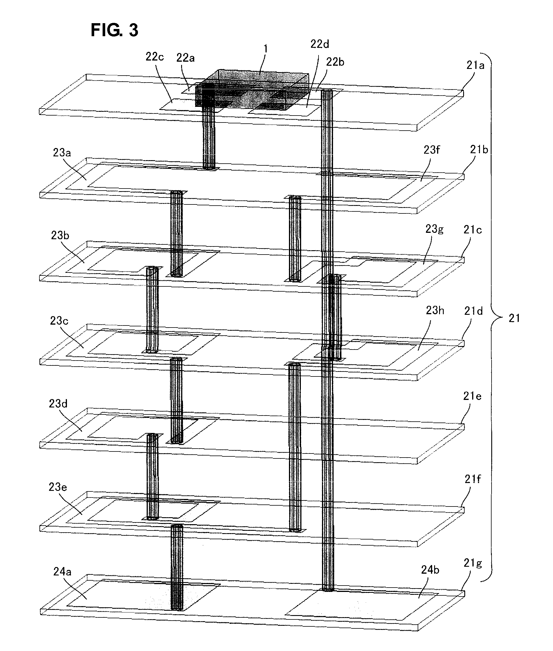
[0067]The functional substrate 20 includes a multilayer substrate 21. On the upper surface of the multilayer substrate 21, mounting electrodes 22a and 22b arranged to mount the wireless IC chip 1 are disposed. In the multilaye...
second preferred embodiment
[0081]FIG. 6 is a plan view illustrating an electrode pattern of a main portion on the upper surface of a radiation plate in a wireless IC device according to the second preferred embodiment of the present invention. On the upper surface of the radiation plate, the long radiation electrodes 32a and 32b and a matching electrode 34 are provided. The matching electrode 34 connects a portion of the radiation electrode 32a apart from the internal end of the radiation electrode 32a by a predetermined distance to a portion of the radiation electrode 32b apart from the internal end of the radiation electrode 32b by the predetermined distance.
[0082]As in the case illustrated in FIG. 2B, near the internal ends of the radiation electrodes 32a and 32, the functional substrate 20 is arranged so that the capacitive coupling electrodes 24a and 24b included in the functional substrate 20 face the internal ends of the radiation electrodes 32a and 32b, respectively. The illustration of the wireless I...
third preferred embodiment
[0084]FIG. 7 is a plan view illustrating an electrode pattern of a main portion on an upper surface of a radiation plate in a wireless IC device according to the third preferred embodiment of the preferred embodiment. On the upper surface of the radiation plate, a loop-shaped radiation electrode 36 is provided. The loop-shaped radiation electrode 36 is preferably arranged so that both ends thereof face each other and it surrounds a predetermined area. The functional substrate 20 is mounted on the radiation plate so that one end of the loop-shaped radiation electrode 36 faces the capacitive coupling electrode 24a included in the functional substrate 20 and the other end of the loop-shaped radiation electrode 36 faces the capacitive coupling electrode 24b included in the functional substrate 20.
[0085]As in the first and second preferred embodiments, a module is obtained by mounting the wireless IC chip on the functional substrate 20. The configuration of the functional substrate 20 ac...
PUM
 Abstract
Description
Claims
Application Information