Plasma doping apparatus

a technology of doping apparatus and plasma, which is applied in the direction of electrical apparatus, electrical discharge tubes, coatings, etc., to achieve the effect of reducing the defective product rate and high throughpu

Inactive Publication Date: 2009-10-29
PANASONIC CORP
View PDF10 Cites 1 Cited by
  • Summary
  • Abstract
  • Description
  • Claims
  • Application Information

AI Technical Summary

Benefits of technology

[0038]In accordance with the present invention, it becomes possible to provide a plasma doping apparatus that comprises a measuring device for inspecting the dose amount in a vacuum container used for carrying out pl

Problems solved by technology

It is thus found that the phenomenon described above causes the issues with the

Method used


Image

  • Plasma doping apparatus
  • Plasma doping apparatus
  • Plasma doping apparatus

Examples


embodiment

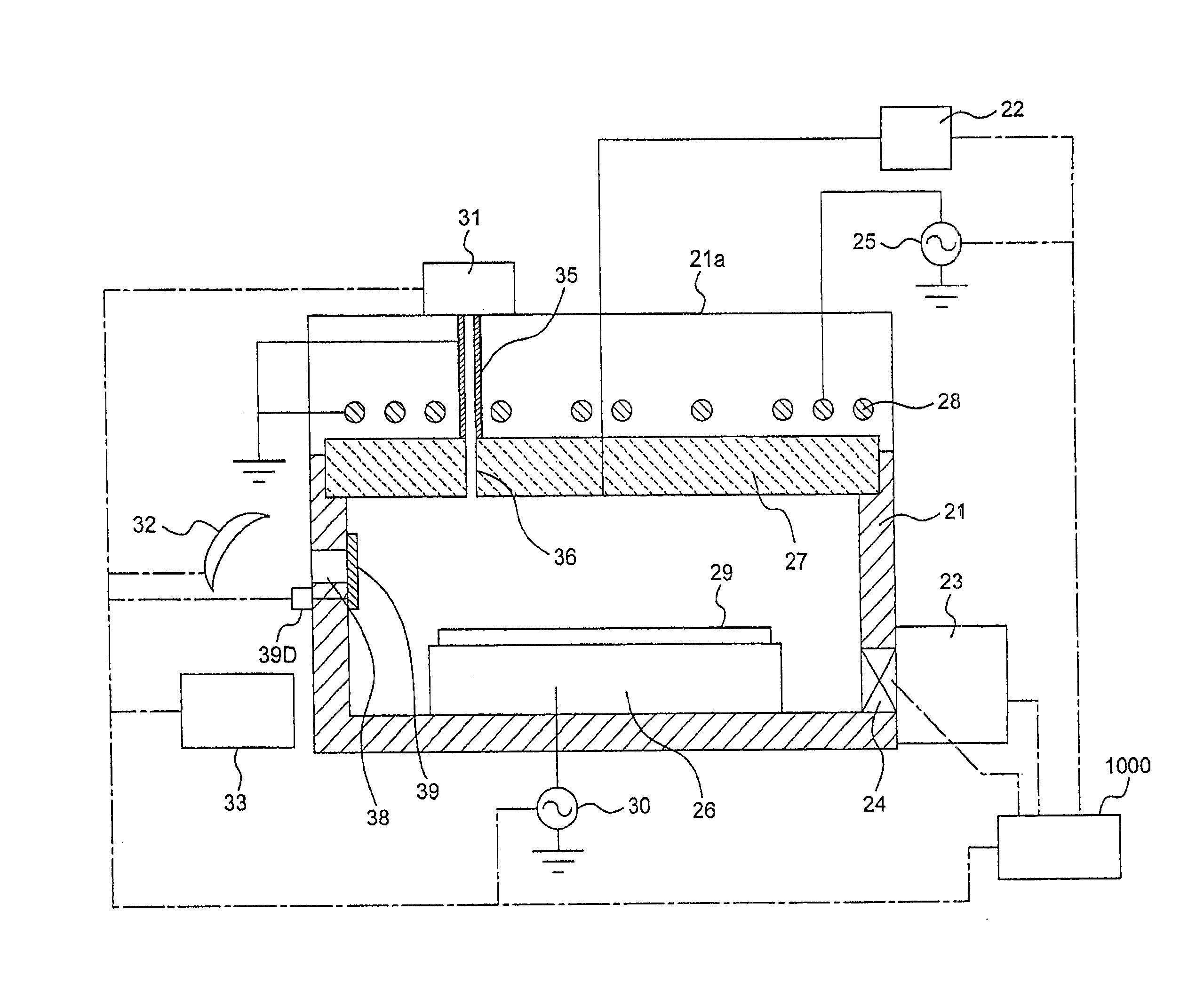
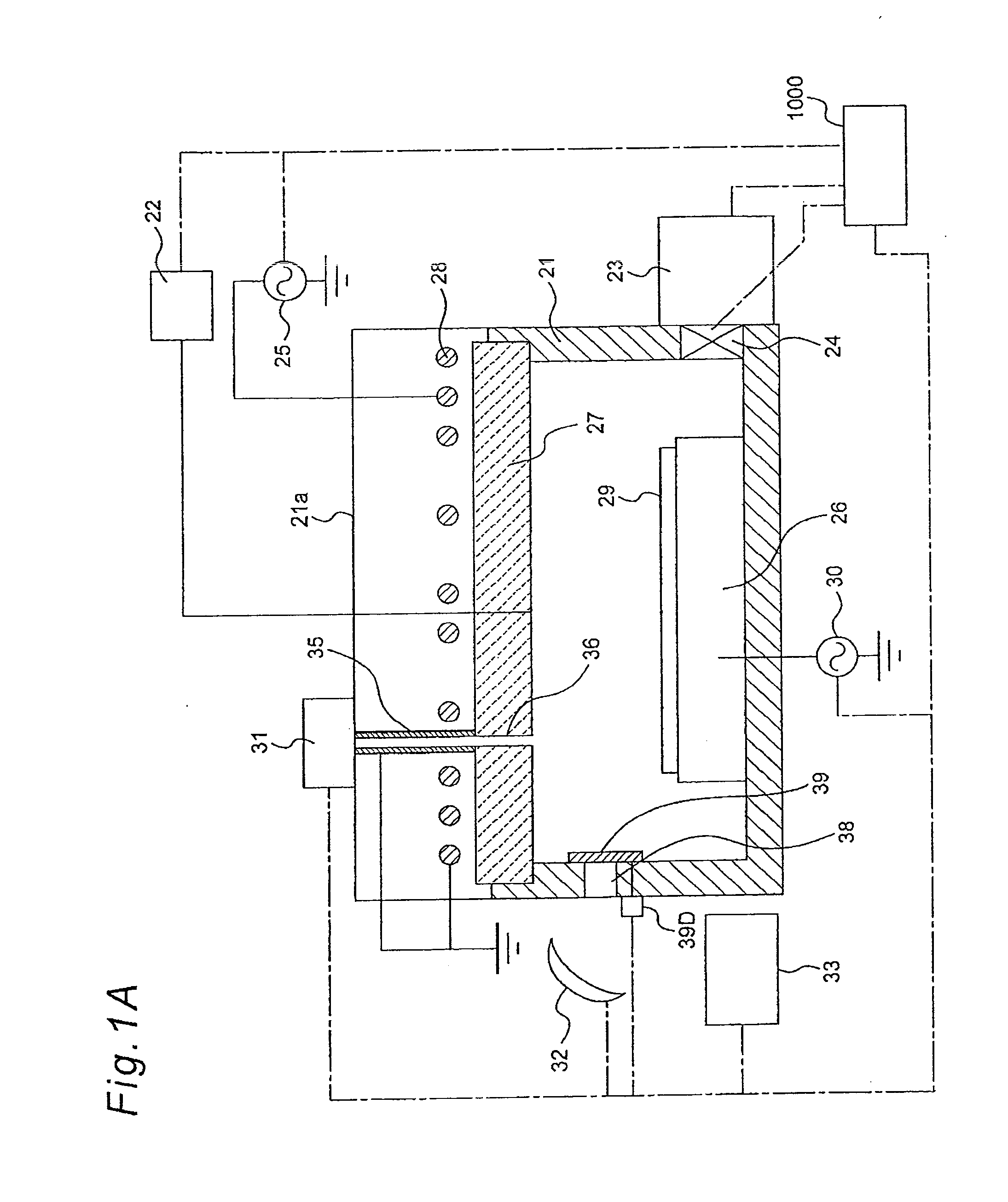
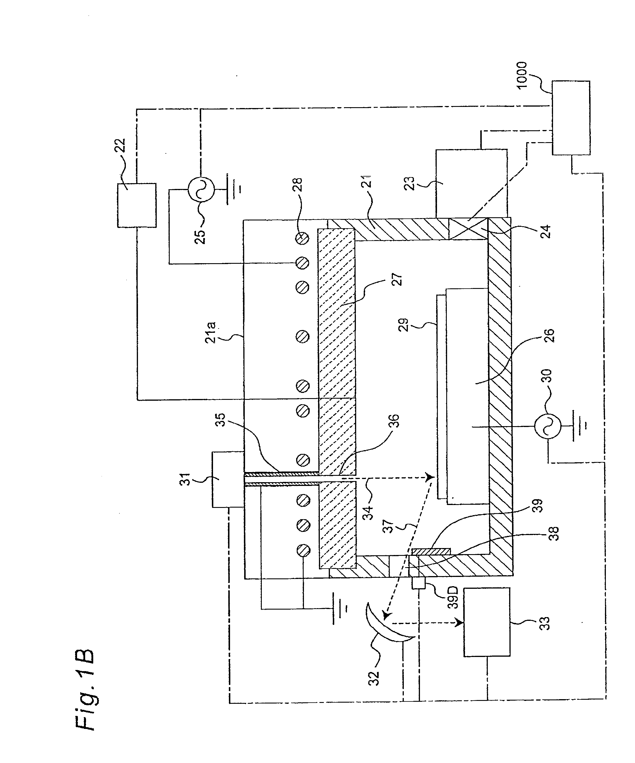
[0054]Referring to FIGS. 1A to 1C and FIG. 2, described below is a plasma doping apparatus in accordance with an embodiment of the present invention.

[0055]FIGS. 1A and 1B are partial cross-sectional views respectively showing a plasma doping apparatus used in one embodiment of the present invention. FIG. 1A shows a state where the shutter 39 to be described later is located at a closed position, and FIG. 1B shows a state where the shutter 39 is located at an open position, respectively.

[0056]In FIGS. 1A and 1B, while B2H6 diluted with He or the like, which serves as a material gas, is being introduced into a vacuum container 21 configuring a vacuum chamber from a gas-supply device 22, exhausting process is carried out by a turbo molecular pump 23 serving as one example of an exhausting device, so that the inside of the vacuum container 21 can be maintained at a predetermined pressure using a pressure-adjusting valve 24. By supplying, using a high-frequency power supply 25, a high-fr...

modified example

[0095]The present invention is not intended to be limited by the aforementioned embodiments, but may be embodied in other various modes.

[0096]For example, as shown in FIG. 1C, the electron beam introducing tube 35 may have a double structure, composed of an outside tube 35A and an inside tube 35B, in which the outside tube 35A is made of metal, such as stainless copper, while the inside tube 35B is made of an insulator.

[0097]With such arrangement, since the materials can be changed between the inner side and the outer side of the electron beam introducing tube 35, the electric potential between the filament 31A and the substrate 29 is easily controlled by the materials, so that the electron beam 34 can be easily transported desirably without reduction in intensity of the electron beam 34. Moreover, since it is possible to reduce a change in the electric field in the electron beam introducing tube 35, which is caused by electromagnetic waves generated by the coil 28, a high-frequency...


PUM


Abstract

On an upper wall of a vacuum container opposing a sample electrode, a plasma-invasion prevention-and-electron beam introducing hole is installed which is communicated with an electron beam introducing tube, and is used for introducing an electron beam toward a substrate in the vacuum container, as well as for preventing invasion of plasma into the electron beam introducing tube. In this structure, supposing that the Debye length of the plasma is set to λd and that a thickness of the sheath is set to Sd, the electron beam introducing hole has a diameter D satisfying a following equation: D≦2λd+2Sd.

Description

BACKGROUND OF THE INVENTION[0001]The present invention relates to a plasma doping apparatus used in a semiconductor device and a manufacturing method thereof, and in particular, used for introducing an impurity into a surface of a solid-state sample such as a semiconductor substrate.[0002]As a technique for introducing an impurity into a surface of a solid-state sample, there has been known a plasma doping method in which the impurity is ionized and introduced into the solid-state sample in a low energy state (for example, see International Publication No. WO / 2006 / 098109 (Japanese Patent Application No. 2005-047598)).[0003]FIG. 5 is a partial cross-sectional view showing a plasma processing apparatus used in a plasma doping method as a conventional impurity introducing method described in International Publication No. WO / 2006 / 098109 (Japanese Patent Application No. 2005-047598). In FIG. 5, while a predetermined gas is being introduced from a gas-supply device 2 into a vacuum contain...

Claims


Application Information

Patent Timeline
IPC IPC(8): B05C11/00
CPCH01J37/32412H01J37/3299H01J37/32935H01J37/32477
Inventor OKASHITA, KATSUMISASAKI, YUICHIROMIZUNO, BUNJI
Owner PANASONIC CORP
Why Eureka
Try Eureka